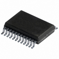
TDA9881TS/V5,118 NXP Semiconductors, TDA9881TS/V5,118 Datasheet - Page 9

TDA9881TS/V5,118
Manufacturer Part Number
TDA9881TS/V5,118
Description
IC IF-PLL DEMOD 24SSOP
Manufacturer
NXP Semiconductors
Type
Demodulatorr
Datasheet
1.TDA9881HNV5118.pdf
(42 pages)
Specifications of TDA9881TS/V5,118
Package / Case
24-SSOP
Applications
Set-Top Boxes
Mounting Type
Surface Mount
Maximum Operating Temperature
+ 70 C
Maximum Power Dissipation
385 mW
Minimum Operating Temperature
- 20 C
Modulation Type
Quadrature
Mounting Style
SMD/SMT
Operating Supply Voltage
5 V
Supply Current
70 A
Lead Free Status / RoHS Status
Lead free / RoHS Compliant
Lead Free Status / RoHS Status
Lead free / RoHS Compliant, Lead free / RoHS Compliant
Other names
935288679118
Philips Semiconductors
9397 750 13417
Product data sheet
8.10 SIF AGC detector
8.7 Video demodulator and amplifier
8.8 Sound carrier trap
8.9 SIF amplifier
The AFC signal is derived from the corresponding downcounter stop value after a
counting cycle. The last four bits are latched and the digital-to-analog converted value is
given as current at pin AFC.
The video demodulator is realized by a multiplier which is designed for low distortion and
large bandwidth. The VIF signal is multiplied with the ‘in phase’ signal of the VIF PLL
VCO.
The demodulator output signal is fed into the video preamplifier via a level shift stage with
integrated low-pass filter to achieve carrier harmonics attenuation.
The output signal of the preamplifier is fed to the VIF AGC detector (see
in the sound trap mode is also fed internally to the integrated sound carrier trap;
see
following postamplifier. The video output level at pin CVBS is 2 V (p-p).
Noise clipping is provided.
The sound carrier trap consists of a reference filter, a phase detector and the sound trap
itself.
A sound carrier reference signal is fed into the reference low-pass filter and is shifted by
nominal 90 degrees. The phase detector compares the original reference signal with the
signal shifted by the reference filter and produces a DC voltage by charging or discharging
an integrated capacitor with a current proportional to the phase difference between both
signals, respectively to the frequency error of the integrated filters. The DC voltage
controls the frequency position of the reference filter and the sound trap. Thus the
accurate frequency position for the different standards is set by the sound carrier
reference signal.
The sound trap itself is constructed of three separate traps to realize sufficient
suppression of the first and second sound carrier.
The SIF amplifier consists of three AC-coupled differential stages. Gain control is
performed by emitter degeneration. The total gain control range is typical 66 dB. The
differential input impedance is typical 2 k in parallel with 3 pF.
SIF gain control is performed by the detection of the SIF voltage at the output of the SIF
amplifier so that a constant SIF signal is supplied to the single reference QSS mixer.
For an optimum adaption between the SIF AGC and the VIF AGC characteristics at 13 dB
picture-to-sound FM carrier ratio, the internal SIF level is reduced.
The integrated AGC capacitor is charged or discharged for the generation of the required
SIF gain via a comparator. An additional circuit (threshold approximately 7 dB) ensures a
very fast gain reduction for a large increasing IF amplitude step.
Section
8.8. The differential trap output signal is converted and amplified by the
Rev. 01 — 16 November 2004
Alignment-free vision and FM sound IF PLL demodulator
© Koninklijke Philips Electronics N.V. 2004. All rights reserved.
TDA9881
Section
8.3) and
9 of 42


