ISL59920IRZ Intersil, ISL59920IRZ Datasheet - Page 12
ISL59920IRZ
Manufacturer Part Number
ISL59920IRZ
Description
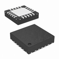
IC ANLG VID LINE TRPL 20-QFN
Manufacturer
Intersil
Type
Video Delay Liner
Datasheet
1.ISL59922IRZ.pdf
(16 pages)
Specifications of ISL59920IRZ
Applications
RGB Video Signals
Mounting Type
Surface Mount
Package / Case
20-VQFN Exposed Pad, 20-HVQFN, 20-SQFN, 20-DHVQFN
Lead Free Status / RoHS Status
Lead free / RoHS Compliant
Available stocks
Company
Part Number
Manufacturer
Quantity
Price
Company:

Part Number:
ISL59920IRZ-T7
Manufacturer:
Intersil
Quantity:
1 050


Figure 32 shows the ISL5992x block diagram. The 3 analog
inputs are ground referenced single-ended signals. After the
signal is received, the delay is introduced by switching filter
blocks into the signal path. Each filter block is an all-pass
filter introducing either 1, 1.5 or 2ns of delay. In addition to
adding delay, each filter block also introduces some low
pass filtering. As a result, the bandwidth of the signal path
decreases from the 0ns delay setting to the maximum delay
setting, as shown in Figures 2 through 9 of the “Typical
Performance Curves”.
In operation, it is best to allocate the most delayed signal
0ns delay then increase the delay on the other channels to
bring them into line. This will result in delay compensation
with the lowest power and distortion.
Serial Bus Operation
The ISL5992x is programmed via 8-bit words sent through
its serial interface. The first bit (MSB) of SDATA is latched on
the first falling clock edge after SENABLE goes low, as
shown in Figure 33. This bit should be a 0 under all
conditions. The next two bits determine the color register to
be written to: 01 = R, 02 = G, and 03 = B (00 is reserved for
the test register). The final five bits set the delay for the
specified color. After 8 bits are latched, any additional clocks
are treated as a new word (data is shifted directly to the final
registers as it is clocked in). This allows the user to write (for
example) the 24 bits of data necessary for R, G, and B as a
single 24-bit word. It is the user's responsibility to send
complete multiples of 8 clock cycles. The serial state
machine is reset on the falling edge of SENABLE, so any
data corruption that may have occurred due to too many or
too few clocks can be corrected with a new word with the
correct number of clocks. The initial value of all registers on
power-up is 0.
vwxyz
00000
00001
00010
00011
*D0 is 0 when addressing the test register
SENABLE
SCLOCK
ISL59920
SDATA
DELAY
TABLE 2. SERIAL BUS DATA
0
2
4
6
ISL59921
DELAY
12
1.5
4.5
0
3
0
ISL59920, ISL59921, ISL59922, ISL59923
t
SEN_SETUP
ISL59922
DELAY
0
1
2
3
A1
a
ISL59923
DELAY
FIGURE 33. SERIAL TIMING
A0
b
0
2
4
6
D4
v
NOTE: Delay register word = 0abvwxyz; Red register - ab = 01;
Green register - ab = 10; Blue register - ab = 11; vwxyz selects
delay; ab = 00 writes to the test register to change the DAC slice
level.
D3
w
vwxyz
00100
00101
01000
01001
01010
10000
10001
10010
10100
10101
00110
00111
01011
01100
01101
01110
10011
10110
10111
11000
11001
11010
11011
11100
11101
01111
11110
11111
TABLE 2. SERIAL BUS DATA (Continued)
D2
x
ISL59920
DELAY
10
12
14
16
18
20
22
24
26
28
30
32
34
36
38
40
42
44
46
48
50
52
54
56
58
60
62
8
D1
y
t
SEN_CYCLE
ISL59921
DELAY
10.5
13.5
16.5
19.5
22.5
25.5
28.5
31.5
34.5
37.5
40.5
43.5
46.5
7.5
12
15
18
21
24
27
30
33
36
39
42
45
6
9
D0*
z
ISL59922
DELAY
10
11
12
13
14
15
16
17
18
19
20
21
22
23
24
25
26
27
28
29
30
31
4
5
6
7
8
9
August 31, 2010
ISL59923
DELAY
N/A
N/A
N/A
N/A
N/A
N/A
N/A
N/A
N/A
N/A
N/A
N/A
N/A
N/A
N/A
N/A
10
12
14
16
18
20
22
24
26
28
30
8
FN6826.2
Related parts for ISL59920IRZ
Image
Part Number
Description
Manufacturer
Datasheet
Request
R

Part Number:
Description:
Intersil Corporation [CMOS Serial Controller Interface]
Manufacturer:
Intersil Corporation
Datasheet:
Part Number:
Description:
Manufacturer:
Intersil Corporation
Datasheet:
Part Number:
Description:
357-036-542-201 CARDEDGE 36POS DL .156 BLK LOPRO
Manufacturer:
Intersil Corporation
Datasheet:
Part Number:
Description:
1024-Word x 4-Bit LSI Static RAM
Manufacturer:
Intersil Corporation
Datasheet:
Part Number:
Description:
General Purpose NPN Transistor Arrays FN341.4
Manufacturer:
Intersil Corporation
Datasheet:
Part Number:
Description:
CMOS 16-Bit Microprocessor
Manufacturer:
Intersil Corporation
Datasheet:
Part Number:
Description:
Manufacturer:
Intersil Corporation
Datasheet:
Part Number:
Description:
Manufacturer:
Intersil Corporation
Datasheet:
Part Number:
Description:
Manufacturer:
Intersil Corporation
Datasheet:
Part Number:
Description:
Manufacturer:
Intersil Corporation
Datasheet:
Part Number:
Description:
CMOS 6-Bit Latch and Decoder Memory Interfaces
Manufacturer:
Intersil Corporation
Datasheet:
Part Number:
Description:
CA3046General Purpose NPN Transistor Arrays
Manufacturer:
Intersil Corporation
Datasheet:
Part Number:
Description:
Manufacturer:
Intersil Corporation
Datasheet:
Part Number:
Description:
TR909 DLC/FLC SLIC with Low Power Standby
Manufacturer:
Intersil Corporation
Datasheet:
Part Number:
Description:
Manufacturer:
Intersil Corporation
Datasheet: