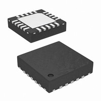
ISL59920IRZ Intersil, ISL59920IRZ Datasheet - Page 4

ISL59920IRZ
Manufacturer Part Number
ISL59920IRZ
Description
IC ANLG VID LINE TRPL 20-QFN
Manufacturer
Intersil
Type
Video Delay Liner
Datasheet
1.ISL59922IRZ.pdf
(16 pages)
Specifications of ISL59920IRZ
Applications
RGB Video Signals
Mounting Type
Surface Mount
Package / Case
20-VQFN Exposed Pad, 20-HVQFN, 20-SQFN, 20-DHVQFN
Lead Free Status / RoHS Status
Lead free / RoHS Compliant
Available stocks
Company
Part Number
Manufacturer
Quantity
Price
Company:
Part Number:
ISL59920IRZ-T7
Manufacturer:
Intersil
Quantity:
1 050
Electrical Specifications
NOTES:
POWER SUPPLY CHARACTERISTICS
V+
V-
I
I
I
I
Δ
I
SERIAL INTERFACE CHARACTERISTICS
t
t
t
PARAMETER
2. The limits for the “Nominal Delay Increment” are derived by taking the limits for the “Maximum Delay” and dividing by the number of steps for the
3. All supply currents measured with Delay R = 0ns, G = mid delay, B = full delay.
4. Offset measurements are referred to 75Ω load as shown in Figure 1.
SP
SPO
SM
SMO
STANDBY
MAX
SEN_SETUP
SEN_CYCLE
I
SP
device. For the ISL59920, ISL59921, and ISL59922 the number of steps is 31; for the ISL59923 the number of steps is 15.
V
IN
FIGURE 1. V
V
V
Positive Supply Current (Note 3)
Positive Output Supply Current (Note 3)
Negative Supply Current (Note 3)
Negative Output Supply Current (Note 3)
Supply Current (Note 3)
Positive Supply Standby Current (Note 3)
Max SCLOCK Frequency
SENABLE to SCLOCK falling edge setup time.
See Figure 33.
Minimum Separation Between SENABLE rising
edge and next SENABLE falling edge. See Figure 33.
SP
SM
x2
, V
, V
-
OS
SPO
SMO
MEASUREMENT CONDITIONS
V
Positive Supply Range
OUT
Negative Supply Range
4
DESCRIPTION
V
R
SP
75Ω
LOAD
= V
ISL59920, ISL59921, ISL59922, ISL59923
= 150Ω on all video outputs, unless otherwise specified. (Continued)
SPO
= +5V, V
75Ω
V
OS
SM
= V
SMP
= -5V, GAIN = 2, T
ISL59920
ISL59921, ISL59922
ISL59923
ISL59920
ISL59921, ISL59922
ISL59923
ISL59920, ISL59921, ISL59922
ISL59923
Increase in I
channel
Chip enable = 0V
Maximum programming clock speed
SENABLE falling edge should occur at least
t
and t
Clock edges occurring within t_en_ck of the
SENABLE falling edge will have
indeterminate effect.
If SENABLE is taken low less than 3µs after it
was taken high, there is a small possibility that
an offset correction will not be initiated.
SEN_SETUP
SEN_SETUP
SP
ns after previous (ignored) clock
per unit step in delay per
CONDITION
before next (desired) clock.
A
= +25°C, exposed die plate = -5V, x2 = 5V,
-35.45 -31
-15.5
-17.5
+4.5
MIN
11.3
11.3
-4.5
9.9
98
98
74
3
TYP MAX
125
115
-13
-13
0.9
2.6
90
13
13
13
10
+5.5
15.3
16.3
-5.5
127
146
106
-9.5
-26
-11
16
10
August 31, 2010
FN6826.2
UNIT
MHz
mA
mA
mA
mA
mA
mA
mA
mA
mA
mA
mA
ns
µs
V
V


