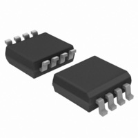
74HCT2G125DC,125 NXP Semiconductors, 74HCT2G125DC,125 Datasheet - Page 2

74HCT2G125DC,125
Manufacturer Part Number
74HCT2G125DC,125
Description
IC BUFF DVR TRI-ST DL 8VSSOP
Manufacturer
NXP Semiconductors
Series
74HCTr
Datasheet
1.74HC2G125DP125.pdf
(14 pages)
Specifications of 74HCT2G125DC,125
Package / Case
US8, 8-VSSOP
Logic Type
Buffer/Line Driver, Non-Inverting
Number Of Elements
2
Number Of Bits Per Element
1
Current - Output High, Low
6mA, 6mA
Voltage - Supply
4.5 V ~ 5.5 V
Operating Temperature
-40°C ~ 125°C
Mounting Type
Surface Mount
Logic Family
HCT
Number Of Channels Per Chip
2
Polarity
Non-Inverting
Supply Voltage (max)
5.5 V
Supply Voltage (min)
4.5 V
Maximum Operating Temperature
+ 125 C
Mounting Style
SMD/SMT
High Level Output Current
- 6 mA
Input Bias Current (max)
20 uA
Low Level Output Current
6 mA
Minimum Operating Temperature
- 40 C
Output Type
3-State
Propagation Delay Time
15 ns (Typ) @ 4.5 V
Number Of Lines (input / Output)
2 / 2
Lead Free Status / RoHS Status
Lead free / RoHS Compliant
Lead Free Status / RoHS Status
Lead free / RoHS Compliant, Lead free / RoHS Compliant
Other names
74HCT2G125DC-G
74HCT2G125DC-G
935274707125
74HCT2G125DC-G
935274707125
NXP Semiconductors
4. Marking
Table 2.
5. Functional diagram
6. Pinning information
74HC_HCT2G125_4
Product data sheet
Type number
74HC2G125DP
74HCT2G125DP
74HC2G125DC
74HCT2G125DC
74HC2G125GD
74HCT2G125GD
Fig 1.
Fig 4.
2
1
5
7
Logic symbol
Pin configuration SOT505-2 (TSSOP8) and
SOT765-1 (VSSOP8)
Marking
1OE
2OE
1A
2A
GND
1OE
1A
2Y
6.1 Pinning
1
2
3
4
mce185
74HCT2G125
74HC2G125
1Y
2Y
6
3
001aae074
8
7
6
5
Fig 2.
V
2OE
1Y
2A
CC
2
1
5
7
Rev. 04 — 4 July 2008
IEC logic symbol
EN1
EN2
74HC2G125; 74HCT2G125
Marking code
H25
T25
H25
T25
H25
T25
mce186
Fig 5.
1
2
6
3
Pin configuration SOT996-2 (XSON8U)
GND
1OE
1A
2Y
1
2
3
4
Fig 3.
Transparent top view
OE
74HCT2G125
74HC2G125
A
Dual buffer/line driver; 3-state
Logic diagram (one driver)
© NXP B.V. 2008. All rights reserved.
001aai333
8
7
6
5
V
2OE
1Y
2A
CC
mna120
2 of 14
Y


