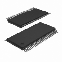
74ALVCH162827DGG,1 NXP Semiconductors, 74ALVCH162827DGG,1 Datasheet - Page 4

74ALVCH162827DGG,1
Manufacturer Part Number
74ALVCH162827DGG,1
Description
IC BUFF DVR TRI-ST 20BIT 56TSSOP
Manufacturer
NXP Semiconductors
Series
74ALVCHr
Datasheet
1.74ALVCH162827DGG1.pdf
(10 pages)
Specifications of 74ALVCH162827DGG,1
Package / Case
56-TSSOP
Logic Type
Buffer/Line Driver, Non-Inverting
Number Of Elements
2
Number Of Bits Per Element
10
Current - Output High, Low
12mA, 12mA
Voltage - Supply
2.3 V ~ 2.7 V
Operating Temperature
-40°C ~ 85°C
Mounting Type
Surface Mount
Logic Family
ALVC
Number Of Channels Per Chip
20
Polarity
Non-Inverting
Supply Voltage (max)
3.6 V
Supply Voltage (min)
2.3 V
Maximum Operating Temperature
+ 85 C
Mounting Style
SMD/SMT
High Level Output Current
- 12 mA
Input Bias Current (max)
40 uA
Low Level Output Current
12 mA
Minimum Operating Temperature
- 40 C
Output Type
3-State
Propagation Delay Time
3.1 ns (Typ) @ 2.7 V or 2.9 ns (Typ) @ 3.3 V
Number Of Lines (input / Output)
20 / 20
Lead Free Status / RoHS Status
Lead free / RoHS Compliant
Lead Free Status / RoHS Status
Lead free / RoHS Compliant, Lead free / RoHS Compliant
Other names
74ALVCH162827DG-T
74ALVCH162827DG-T
935254370118
74ALVCH162827DG-T
935254370118
1. The input and output voltage ratings may be exceeded if the input and output current ratings are observed.
Philips Semiconductors
LOGIC DIAGRAM
RECOMMENDED OPERATING CONDITIONS
ABSOLUTE MAXIMUM RATINGS
In accordance with the Absolute Maximum Rating System (IEC 134)
Voltages are referenced to GND (ground = 0V)
NOTE:
1998 Sep 29
SYMBOL
20-bit buffer/line driver, non-inverting, with 30
termination resistors (3-State)
nOE1
nOE2
SYMBOL
I
GND
T
V
V
t
P
V
amb
r
V
V
T
I
CC
CC
, t
V
I
TOT
O
V
OK
I
CC
IK
stg
I
O
O
, I
f
I
CC
DC supply voltage 2.5V range (for max. speed
performance @ 30 pF output load)
DC supply voltage 3.3V range (for max. speed
performance @ 50 pF output load)
DC Input voltage range
DC output voltage range
Operating free-air temperature range
Input rise and fall times
DC supply voltage
DC input diode current
DC input voltage
DC output diode current
DC output voltage
DC output source or sink current
DC V
Storage temperature range
Power dissipation per package
–plastic thin-medium-shrink (TSSOP)
nY0
nA0
CC
or GND current
PARAMETER
PARAMETER
nY1
nA1
nY2
nA2
V
Note 1
V
Note 1
V
For temperature range: –40 to +125 C
above +55 C derate linearly with 8 mW/K
I
O
O
t0
nY3
nA3
uV
= 0 to V
CC
or V
CC
4
V
V
O
nY4
CC
CC
nA4
CONDITIONS
CONDITIONS
t 0
= 2.3 to 3.0V
= 3.0 to 3.6V
nA5
nY5
nA6
nY6
MIN
–40
2.3
3.0
0
0
0
0
–0.5 to V
74ALVCH162827
nY7
nA7
–0.5 to +4.6
–0.5 to +4.6
–65 to +150
RATING
"100
"50
"50
–50
600
MAX
V
V
+85
2.7
3.6
CC
20
10
CC
CC
+0.5
Product specification
nY8
nA8
SH00013
UNIT
ns/V
UNIT
mW
mA
mA
mA
mA
V
V
V
V
C
V
V
V
C
nA9
nY9


