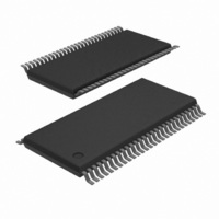
74ALVCH16827DGG,11 NXP Semiconductors, 74ALVCH16827DGG,11 Datasheet - Page 7

74ALVCH16827DGG,11
Manufacturer Part Number
74ALVCH16827DGG,11
Description
IC BUFF DVR TRI-ST 20BIT 56TSSOP
Manufacturer
NXP Semiconductors
Series
74ALVCHr
Datasheet
1.74ALVCH16827DGG11.pdf
(10 pages)
Specifications of 74ALVCH16827DGG,11
Package / Case
56-TSSOP
Logic Type
Buffer/Line Driver, Non-Inverting
Number Of Elements
2
Number Of Bits Per Element
10
Current - Output High, Low
24mA, 24mA
Voltage - Supply
1.2 V ~ 3.6 V
Operating Temperature
-40°C ~ 85°C
Mounting Type
Surface Mount
Logic Family
ALVC
Number Of Channels Per Chip
20
Polarity
Non-Inverting
Supply Voltage (max)
3.6 V
Supply Voltage (min)
2.3 V
Maximum Operating Temperature
+ 85 C
Mounting Style
SMD/SMT
High Level Output Current
- 24 mA
Input Bias Current (max)
40 uA
Low Level Output Current
24 mA
Minimum Operating Temperature
- 40 C
Output Type
3-State
Propagation Delay Time
2.1 ns (Typ) @ 2.7 V or 2 ns (Typ) @ 3.3 V
Number Of Lines (input / Output)
20 / 20
Lead Free Status / RoHS Status
Lead free / RoHS Compliant
Lead Free Status / RoHS Status
Lead free / RoHS Compliant, Lead free / RoHS Compliant
Other names
74ALVCH16827DG-T
74ALVCH16827DG-T
935254390118
74ALVCH16827DG-T
935254390118
Philips Semiconductors
AC WAVEFORMS FOR V
V
V
V
V
V
output load.
AC WAVEFORMS FOR V
V
V
V
V
V
output load.
V
V
1998 Jul 27
I
I
M
X
Y
OL
M
X
Y
OL
CC
CC
= 2.7V
= V
20-bit buffer/line driver, non-inverting (3-State)
OUTPUT
LOW-to-OFF
OFF-to-LOW
OUTPUT
HIGH-to-OFF
OFF-to-HIGH
Waveform 2. The 3-State Output Enable and Disable Times
= V
= V
= V
= V
nOE INPUT
Waveform 1. The Input (nAx) to Output (nYx) Propagation
= 0.5 V
= 1.5 V
and V
and V
GND
V
V
V
A
INPUT
GND
V
Y
OUTPUT
V
V
GND
< 2.3V RANGE
= 2.7V RANGE
CC
V
OL
OH
I
n
OH
n
OL
CC
OL
OH
OL
OH
I
+ 0.15V
+ 0.3V
–0.15V
–0.3V
OH
OH
are the typical output voltage drop that occur with the
are the typical output voltage drop that occur with the
V
outputs
enabled
V
M
t
M
PHL
t
PLZ
t
PHZ
V
Delays
M
CC
CC
V
X
V
Y
= 2.3V TO 2.7V AND
= 3.0V TO 3.6V AND
outputs
disabled
t
t
PZL
PLH
t
PZH
V
SH00132
M
SH00137
V
M
outputs
enabled
7
TEST CIRCUIT
GENERATOR
t
t
PLZ/
PHZ/
PULSE
SWITCH POSITION
t
PLH/
TEST
DEFINITIONS
R
C
R
Waveform 3. Load circuitry for switching times
t
t
L
L
T
PZL
PZH
t
= Load resistor
= Load capacitance includes jig and probe capacitance
= Termination resistance should be equal to Z
PHL
Test Circuit for switching times
2 < V
Open
V
GND
I
S
1
R
T
CC
D.U.T.
V
CC
2.7–3.6V
< 2.7V
74ALVCH16827
V
CC
V
O
C
L
OUT
2.7V
V
V
Product specification
CC
I
of pulse generators.
S
1
R
R
SV00906
L
L
= 500
= 500
2 * V
Open
GND
CC


