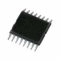
74LVC169PW,112 NXP Semiconductors, 74LVC169PW,112 Datasheet - Page 11

74LVC169PW,112
Manufacturer Part Number
74LVC169PW,112
Description
IC SYNC 4BIT BIN COUNTER 16TSSOP
Manufacturer
NXP Semiconductors
Series
74LVCr
Type
Binaryr
Datasheet
1.74LVC169D112.pdf
(22 pages)
Specifications of 74LVC169PW,112
Package / Case
16-TSSOP
Logic Type
Binary Counter
Direction
Up, Down
Number Of Elements
1
Number Of Bits Per Element
4
Timing
Synchronous
Count Rate
150MHz
Trigger Type
Positive Edge
Voltage - Supply
2.7 V ~ 3.6 V
Operating Temperature
-40°C ~ 125°C
Mounting Type
Surface Mount
Mounting Style
SMD/SMT
Technology
CMOS
Number Of Elements
1
Number Of Bits
4
Logic Family
LVC
Logical Function
Counter
Operating Supply Voltage (typ)
1.8/2.5/3.3V
Output Type
Standard
Package Type
TSSOP
Propagation Delay Time
11ns
Operating Temp Range
-40C to 125C
Operating Supply Voltage (min)
1.2V
Operating Supply Voltage (max)
3.6V
Operating Temperature Classification
Automotive
Mounting
Surface Mount
Pin Count
16
Lead Free Status / RoHS Status
Lead free / RoHS Compliant
Reset
-
Lead Free Status / Rohs Status
Compliant
Other names
74LVC169PW
74LVC169PW
935210590112
74LVC169PW
935210590112
NXP Semiconductors
Table 7.
Voltages are referenced to GND (ground = 0 V). For test circuit see
[1]
[2]
[3]
[4]
11. Waveforms
74LVC169_5
Product data sheet
Symbol Parameter
f
t
C
max
sk(0)
Fig 8.
PD
Typical values are measured at T
t
Skew between any two outputs of the same package switching in the same direction. This parameter is guaranteed by design.
C
P
f
C
V
N = number of inputs switching
pd
i
D
CC
PD
= input frequency in MHz; f
L
(C
is the same as t
= output load capacitance in pF
= C
L
is used to determine the dynamic power dissipation (P
= supply voltage in V
maximum
frequency
output skew time
power dissipation
capacitance
Measurement points are given in
Logic levels: V
Clock (CP) to outputs (Qn, TC) propagation delays, the clock pulse width, and the maximum frequency
PD
V
Dynamic characteristics
CC
2
V
CC
f
o
2
) = sum of outputs
PLH
f
i
OL
N + (C
and t
and V
PHL
Qn, TC output
o
CP input
OH
= output frequency in MHz
Conditions
see
V
per input pin; V
L
.
CC
amb
are the typical output voltage levels that occur with the output load.
V
V
V
V
CC
CC
CC
Figure 8
CC
= 3.0 V to 3.6 V
= 25 C and V
…continued
2
= 2.7 V
= 3.0 V to 3.6 V
= 3.0 V to 3.6 V
GND
V
V
Table
OH
OL
V
f
o
I
) where:
8.
I
= GND to V
CC
Rev. 05 — 8 June 2009
V
= 1.2 V, 1.8 V, 2.5 V, 2.7 V, and 3.3 V respectively.
M
t
PHL
t
W
D
in W).
Presettable synchronous 4-bit up/down binary counter
CC
1/f
V
M
max
[3]
[4]
Figure
Min
150
150
-
-
13.
40 C to +85 C
Typ
t
PLH
200
20
-
-
[1]
001aaa651
Max
1.0
-
-
-
40 C to +125 C Unit
Min
150
150
-
-
74LVC169
© NXP B.V. 2009. All rights reserved.
Max
1.5
-
-
-
11 of 22
MHz
MHz
ns
pF


