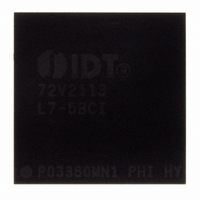
IDT72V2113L7-5BCI IDT, Integrated Device Technology Inc, IDT72V2113L7-5BCI Datasheet - Page 13

IDT72V2113L7-5BCI
Manufacturer Part Number
IDT72V2113L7-5BCI
Description
IC FIFO SYNC 3.3V 5NS 100-LBGA
Manufacturer
IDT, Integrated Device Technology Inc
Series
72Vr
Datasheet
1.IDT72V2103L15PF8.pdf
(46 pages)
Specifications of IDT72V2113L7-5BCI
Function
Synchronous
Memory Size
4.7Mb (262k x 18)
Access Time
5ns
Voltage - Supply
3.15 V ~ 3.45 V
Operating Temperature
-40°C ~ 85°C
Mounting Type
Surface Mount
Package / Case
100-LBGA
Configuration
Dual
Density
4.5Mb
Access Time (max)
5ns
Word Size
18/9Bit
Organization
256Kx18/512Kx9
Sync/async
Synchronous
Expandable
Yes
Bus Direction
Uni-Directional
Clock Freq (max)
133.3MHz
Operating Supply Voltage (typ)
3.3V
Operating Supply Voltage (min)
3.15V
Operating Supply Voltage (max)
3.45V
Supply Current
35mA
Operating Temp Range
-40C to 85C
Operating Temperature Classification
Industrial
Mounting
Surface Mount
Pin Count
100
Lead Free Status / RoHS Status
Contains lead / RoHS non-compliant
Data Rate
-
Lead Free Status / RoHS Status
Not Compliant, Contains lead / RoHS non-compliant
Other names
72V2113L7-5BCI
800-1513
800-1513
Available stocks
Company
Part Number
Manufacturer
Quantity
Price
Company:
Part Number:
IDT72V2113L7-5BCI
Manufacturer:
IDT, Integrated Device Technology Inc
Quantity:
10 000
PROGRAMMING FLAG OFFSETS
72V2113 has internal registers for these offsets. There are eight default offset
values selectable during Master Reset. These offset values are shown in Table
2. Offset values can also be programmed into the FIFO in one of two ways; serial
or parallel loading method. The selection of the loading method is done using
the LD (Load) pin. During Master Reset, the state of the LD input determines
whether serial or parallel flag offset programming is enabled. A HIGH on LD
during Master Reset selects serial loading of offset values. A LOW on LD during
Master Reset selects parallel loading of offset values.
the current offset values. Offset values can be read via the parallel output port
Q0-Qn, regardless of the programming mode selected (serial or parallel). It is
not possible to read the offset values in serial fashion.
TABLE 2 — DEFAULT PROGRAMMABLE
FLAG OFFSETS
NOTES:
1. n = empty offset for PAE.
2. m = full offset for PAF.
3. As well as selecting serial programming mode, one of the default values will also
4. As well as selecting parallel programming mode, one of the default values will
IDT72V263/273/283/293/103/113 3.3V HIGH DENSITY SUPERSYNC II
8K x 18, 16K x 9/18, 32K x 9/18, 64K x 9/18, 128K x 9/18, 256K x 9/18, 512K x9
IDT72V2103/72V2113 3.3V HIGH DENSITY SUPERSYNC II
131,072 x 18/262,144 x 9, 262,144 x 18/524,288 x 9
be loaded depending on the state of FSEL0 & FSEL1.
also be loaded depending on the state of FSEL0 & FSEL1.
Full and Empty Flag offset values are user programmable. The IDT72V2103/
In addition to loading offset values into the FIFO, it is also possible to read
LD
LD
H
H
H
H
H
L
L
L
L
L
IDT72V2103, IDT72V2113
FSEL0
FSEL0
H
H
H
H
X
X
L
L
L
L
FSEL1
FSEL1
H
H
H
H
X
X
L
L
L
L
Program Mode
Offsets n,m
TM
Parallel
Serial
16,383
8,191
4,095
2,047
1,023
NARROW BUS FIFO
255
127
511
(3)
(4)
TM
13
NARROW BUS FIFO
the control pins and sequence for both serial and parallel programming modes.
For a more detailed description, see discussion that follows.
Master Reset, regardless of whether serial or parallel programming has been
selected. Valid programming ranges are from 0 to D-1.
SYNCHRONOUS vs ASYNCHRONOUS PROGRAMMABLE FLAG
TIMING SELECTION
cycle with either synchronous or asynchronous timing for PAF and PAE flags
by use of the PFM pin.
MRS), the PAF is asserted and updated on the rising edge of WCLK only and
not RCLK. Similarly, PAE is asserted and updated on the rising edge of RCLK
only and not WCLK. For detail timing diagrams, see Figure 18 for synchronous
PAF timing and Figure 19 for synchronous PAE timing.
MRS), the PAF is asserted LOW on the LOW-to-HIGH transition of WCLK and
PAF is reset to HIGH on the LOW-to-HIGH transition of RCLK. Similarly, PAE
is asserted LOW on the LOW-to-HIGH transition of RCLK. PAE is reset to HIGH
on the LOW-to-HIGH transition of WCLK. For detail timing diagrams, see Figure
20 for asynchronous PAF timing and Figure 21 for asynchronous PAE timing.
Figure 3, Programmable Flag Offset Programming Sequence, summaries
The offset registers may be programmed (and reprogrammed) any time after
The IDT72V2103/72V2113 can be configured during the Master Reset
If synchronous PAF/PAE configuration is selected (PFM, HIGH during
If asynchronous PAF/PAE configuration is selected (PFM, LOW during
COMMERCIAL AND INDUSTRIAL
TEMPERATURE RANGES
JUNE 1, 2010


