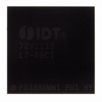
IDT72V2113L7-5BCI IDT, Integrated Device Technology Inc, IDT72V2113L7-5BCI Datasheet - Page 9

IDT72V2113L7-5BCI
Manufacturer Part Number
IDT72V2113L7-5BCI
Description
IC FIFO SYNC 3.3V 5NS 100-LBGA
Manufacturer
IDT, Integrated Device Technology Inc
Series
72Vr
Datasheet
1.IDT72V2103L15PF8.pdf
(46 pages)
Specifications of IDT72V2113L7-5BCI
Function
Synchronous
Memory Size
4.7Mb (262k x 18)
Access Time
5ns
Voltage - Supply
3.15 V ~ 3.45 V
Operating Temperature
-40°C ~ 85°C
Mounting Type
Surface Mount
Package / Case
100-LBGA
Configuration
Dual
Density
4.5Mb
Access Time (max)
5ns
Word Size
18/9Bit
Organization
256Kx18/512Kx9
Sync/async
Synchronous
Expandable
Yes
Bus Direction
Uni-Directional
Clock Freq (max)
133.3MHz
Operating Supply Voltage (typ)
3.3V
Operating Supply Voltage (min)
3.15V
Operating Supply Voltage (max)
3.45V
Supply Current
35mA
Operating Temp Range
-40C to 85C
Operating Temperature Classification
Industrial
Mounting
Surface Mount
Pin Count
100
Lead Free Status / RoHS Status
Contains lead / RoHS non-compliant
Data Rate
-
Lead Free Status / RoHS Status
Not Compliant, Contains lead / RoHS non-compliant
Other names
72V2113L7-5BCI
800-1513
800-1513
Available stocks
Company
Part Number
Manufacturer
Quantity
Price
Company:
Part Number:
IDT72V2113L7-5BCI
Manufacturer:
IDT, Integrated Device Technology Inc
Quantity:
10 000
NOTES:
1. All AC timings apply to both Standard IDT mode and First Word Fall Through mode.
2. Industrial temperature range product for the 7-5ns and 10ns are available as a standard device. All other speed grades are available by special order.
3. Pulse widths less than minimum values are not allowed.
4. Values guaranteed by design, not currently tested.
5. TQFP package only: for speed grades 7-5ns, 10ns and 15ns the minimum for t
AC ELECTRICAL CHARACTERISTICS
(Commercial: V
IDT72V263/273/283/293/103/113 3.3V HIGH DENSITY SUPERSYNC II
8K x 18, 16K x 9/18, 32K x 9/18, 64K x 9/18, 128K x 9/18, 256K x 9/18, 512K x9
Symbol
IDT72V2103/72V2113 3.3V HIGH DENSITY SUPERSYNC II
131,072 x 18/262,144 x 9, 262,144 x 18/524,288 x 9
f
t
t
t
t
t
t
t
t
t
t
t
t
t
t
t
t
t
t
t
t
t
t
t
t
t
t
t
S
A
CLK
CLKH
DS
DH
ENH
LDS
LDH
RS
RSR
CLKL
ENS
RSS
RSF
RTS
OLZ
OE
OHZ
WFF
REF
PAFA
PAFS
PAEA
PAES
HF
SKEW1
SKEW2
Clock Cycle Frequency
Data Access Time
Clock Cycle Time
Clock High Time
Clock Low Time
Data Setup Time
Data Hold Time
Enable Setup Time
Enable Hold Time
Load Setup Time
Load Hold Time
Reset Pulse Width
Reset Setup Time
Reset Recovery Time
Reset to Flag and Output Time
Retransmit Setup Time
Output Enable to Output in Low Z
Output Enable to Output Valid
Output Enable to Output in High Z
Write Clock to FF or IR
Read Clock to EF or OR
Clock to Asynchronous Programmable Almost-Full Flag
Write Clock to Synchronous Programmable Almost-Full Flag
Clock to Asynchronous Programmable Almost-Empty Flag
Read Clock to Synchronous Programmable Almost-Empty Flag
Clock to HF
Skew time between RCLK and WCLK for EF/OR and FF/IR
Skew time between RCLK and WCLK for PAE and PAF
CC
= 3.3V ± 0.15V, T
(5)
(3)
Parameter
A
(5)
= 0°C to +70°C; Industrial: V
(4)
(4,5)
TM
NARROW BUS FIFO
CC
= 3.3V ± 0.15V, T
(1)
A
IDT72V2103L6
IDT72V2113L6
Min.
BGA & TQFP
, t
Commercial
TM
2.7
2.7
0.5
0.5
0.5
—
10
15
10
—
—
—
—
—
—
—
—
1
6
2
2
3
3
0
1
1
4
5
OE
9
NARROW BUS FIFO
, and t
Max.
166
OHZ
—
—
—
—
—
—
—
—
—
—
—
—
15
—
—
10
10
10
—
—
4
4
4
4
4
4
4
is 2ns.
A
IDT72V2103L7-5
IDT72V2113L7-5
Com’l & Ind’l
= -40°C to +85°C; JEDEC JESD8-A compliant)
BGA & TQFP
Min.
1
7.5
3.5
3.5
2.5
0.5
2.5
0.5
3.5
0.5
3.5
1
1
—
10
15
10
—
—
—
—
—
—
—
—
0
5
7
(5)
(5)
(5)
133.3
Max.
12.5
12.5
12.5
—
—
—
—
—
—
—
—
—
—
—
—
15
—
—
—
—
5
6
6
5
5
5
5
(2)
IDT72V2103L10
IDT72V2113L10
Com’l & Ind’l
Min.
1
4.5
4.5
3.5
0.5
3.5
0.5
3.5
0.5
3.5
1
1
10
10
15
10
—
—
—
—
—
—
—
—
10
—
TQFP Only
0
7
(5)
(5)
(5)
COMMERCIAL AND INDUSTRIAL
Max.
100
6.5
6.5
6.5
6.5
6.5
—
—
—
—
—
—
—
—
—
—
—
—
15
—
—
16
16
16
—
—
6
6
(2)
TEMPERATURE RANGES
IDT72V2103L15
IDT72V2113L15
Min.
1
1
1
—
15
15
15
15
—
—
—
—
—
—
—
—
14
Commercial
TQFP Only
6
6
4
1
4
1
4
1
4
0
9
(5)
(5)
(5)
JUNE 1, 2010
66.7
Max.
10
—
—
—
—
—
—
—
—
—
—
—
—
15
—
—
10
10
20
10
20
10
20
—
—
8
8
MHz
Unit
ns
ns
ns
ns
ns
ns
ns
ns
ns
ns
ns
ns
ns
ns
ns
ns
ns
ns
ns
ns
ns
ns
ns
ns
ns
ns
ns


