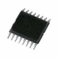
74LVC109PW,112 NXP Semiconductors, 74LVC109PW,112 Datasheet - Page 7

74LVC109PW,112
Manufacturer Part Number
74LVC109PW,112
Description
IC DUAL JK F-F POS-EDGE 16TSSOP
Manufacturer
NXP Semiconductors
Series
74LVCr
Type
JK Typer
Datasheet
1.74LVC109DB118.pdf
(18 pages)
Specifications of 74LVC109PW,112
Output Type
Differential
Package / Case
16-TSSOP
Function
Set(Preset) and Reset
Number Of Elements
2
Number Of Bits Per Element
1
Frequency - Clock
150MHz
Trigger Type
Positive Edge
Current - Output High, Low
24mA, 24mA
Voltage - Supply
2.7 V ~ 3.6 V
Operating Temperature
-40°C ~ 125°C
Mounting Type
Surface Mount
Number Of Circuits
2
Logic Family
LVC
Logic Type
J-K Positive Edge Triggered Flip Flop
Polarity
Inverting/Non-Inverting
Input Type
Single-Ended
Propagation Delay Time
4 ns at 3.3 V
High Level Output Current
- 24 mA
Low Level Output Current
24 mA
Supply Voltage (max)
3.6 V
Maximum Operating Temperature
+ 125 C
Mounting Style
SMD/SMT
Minimum Operating Temperature
- 40 C
Supply Voltage (min)
1.2 V
Technology
CMOS
Number Of Bits
2
Number Of Elements
2
Clock-edge Trigger Type
Positive-Edge
Operating Supply Voltage (typ)
1.8/2.5/3.3V
Package Type
TSSOP
Frequency (max)
225MHz
Operating Supply Voltage (min)
1.2V
Operating Supply Voltage (max)
3.6V
Operating Temp Range
-40C to 125C
Operating Temperature Classification
Automotive
Mounting
Surface Mount
Pin Count
16
Lead Free Status / RoHS Status
Lead free / RoHS Compliant
Delay Time - Propagation
-
Lead Free Status / Rohs Status
Compliant
Other names
74LVC109PW
74LVC109PW
935191070112
74LVC109PW
935191070112
Philips Semiconductors
DC CHARACTERISTICS
At recommended operating conditions; voltages are referenced to GND (ground = 0 V).
2004 Mar 18
T
V
V
V
V
I
I
SYMBOL
LI
CC
amb
I
IH
IL
OH
OL
Dual JK flip-flop with set and reset;
positive-edge trigger
CC
= 40 to 85 C; note 1
HIGH-level input
voltage
LOW-level input
voltage
HIGH-level output
voltage
LOW-level output
voltage
input leakage current
quiescent supply
current
additional quiescent
supply current per
input pin
PARAMETER
V
V
V
V
I
V
I
O
O
I
I
I
I
I
I
I
I
I
I
I
I
= V
= V
= 5.5 V or GND
= V
= 0 A
= V
= 0 A
O
O
O
O
O
O
O
= 100 A
= 12 mA
= 12 mA
= 24 mA
= 100 A
= 12 mA
= 24 mA
IH
IH
CC
CC
OTHER
or V
or V
TEST CONDITIONS
or GND;
0.6 V;
IL
IL
7
1.2
2.7 to 3.6
1.2
2.7 to 3.6
2.7 to 3.6
2.7
3.0
3.0
2.7 to 3.6
2.7
3.0
3.6
3.6
2.7 to 3.6
V
CC
(V)
V
2.0
V
V
V
V
CC
CC
CC
CC
CC
MIN.
0.2
0.5
0.6
0.8
V
GND
0.1
5
0.1
CC
TYP.
Product specification
GND
0.8
0.2
0.4
0.55
10
500
74LVC109
5
MAX.
V
V
V
V
V
V
V
V
V
V
V
UNIT
A
A
A


