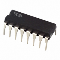
HEF4521BP,652 NXP Semiconductors, HEF4521BP,652 Datasheet - Page 5

HEF4521BP,652
Manufacturer Part Number
HEF4521BP,652
Description
IC FREQ DIVIDER 24STG 16DIP
Manufacturer
NXP Semiconductors
Series
4000Br
Type
D-Type Busr
Specifications of HEF4521BP,652
Package / Case
16-DIP (0.300", 7.62mm)
Function
Master Reset
Output Type
Non-Inverted
Number Of Elements
1
Number Of Bits Per Element
24
Frequency - Clock
35MHz
Delay Time - Propagation
25ns
Trigger Type
Negative Edge
Mounting Type
Through Hole
Mounting Style
SMD/SMT
Dc
07+
Lead Free Status / RoHS Status
Lead free / RoHS Compliant
Voltage - Supply
-
Operating Temperature
-
Current - Output High, Low
-
Lead Free Status / Rohs Status
Lead free / RoHS Compliant
Other names
933406750652
HEF4521BPN
HEF4521BPN
HEF4521BPN
HEF4521BPN
NXP Semiconductors
8. Functional Test
Table 4.
[1]
9. Limiting values
Table 5.
In accordance with the Absolute Maximum Rating System (IEC 60134).
[1]
[2]
HEF4521B_5
Product data sheet
Inputs
MR
H
L
L
L
L
L
Symbol
V
I
V
I
I
I
T
T
P
P
IK
OK
I/O
DD
stg
amb
DD
I
tot
H = HIGH voltage level; L = LOW voltage level;
For DIP16 package: P
For SO16 package: P
A2
L
see
Remarks
column
L
H
H
Functional test sequence
Limiting values
Parameter
supply voltage
input clamping current
input voltage
output clamping current
input/output current
supply current
storage temperature
ambient temperature
total power dissipation
power dissipation
Control terminals
Y2
L
see
Remarks
column
L
L
L
tot
tot
A test function has been included to reduce the test time required to test all 24 counter
stages. This test function divides the counter into three 8-stage sections by connecting
V
parallel via A2 (connected to Y2). All flip-flops are now at a HIGH level. The counter is now
returned to the normal 24-stage in series configuration by connecting V
V
an all HIGH state to an all LOW state.
derates linearly with 8 mW/K above 70 C.
derates linearly with 12 mW/K above 70 C.
SS1
DD1
V
V
V
V
V
V
V
to V
to V
SS1
DD
DD
SS
SS
SS
SS
DD
DD
V
V
V
V
V
V
V
. Entering one more pulse into input A2 will cause the counter to ripple from
and V
DD1
SS
SS
SS
SS
DD
DD
DD1
Outputs
Q18 to Q24
L
H
H
H
H
L
Conditions
V
V
to any supply terminal
DIP16 package
SO16 package
per output
I
O
< 0.5 V or V
= HIGH to LOW transition.
Rev. 05 — 5 November 2009
< 0.5 V or V
to V
SS
. 255 counts are loaded into each of the 8-stage sections in
Remarks
counter is in three 8-stage sections in parallel mode; A2 and Y2
are interconnected (Y2 is now input); counter is reset by MR.
255 pulses are clocked into A2, Y2. The counter advances on
the LOW to HIGH transition.
V
the input A2 is made HIGH.
V
becomes an output; the device is now in the 2
counter ripples from an all HIGH state to an all LOW state.
SS1
DD1
I
O
> V
> V
is connected to V
is connected to V
DD
DD
+ 0.5 V
+ 0.5 V
24-stage frequency divider and oscillator
SS
DD
[1]
[2]
.
; Y2 is now made floating and
Min
-
-
-
-
-
-
-
0.5
0.5
65
40
HEF4521B
Max
V
+150
+18
100
+85
750
500
100
DD
10
10
10
© NXP B.V. 2009. All rights reserved.
SS1
24
+ 0.5
mode.
to V
SS
Unit
V
mA
V
mA
mA
mA
mW
mW
mW
C
C
and
5 of 17


