74VCXH16374TTR STMicroelectronics, 74VCXH16374TTR Datasheet
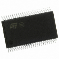
IC FLIP FLOP 16BIT LV D 48-TSSOP

74VCXH16374TTR

Manufacturer Part Number
74VCXH16374TTR
Description
IC FLIP FLOP 16BIT LV D 48-TSSOP
Manufacturer
STMicroelectronics
Series
74VCXHr
Type
D-Type Busr
Datasheet

Specifications of 74VCXH16374TTR

Function
Standard
Output Type
Tri-State Non Inverted
Number Of Elements
2
Number Of Bits Per Element
8
Frequency - Clock
235MHz
Delay Time - Propagation
1ns
Trigger Type
Positive Edge
Current - Output High, Low
24mA, 24mA
Voltage - Supply
2.3 V ~ 3.6 V
Operating Temperature
-55°C ~ 125°C
Mounting Type
Surface Mount
Package / Case
48-TSSOP
Lead Free Status / RoHS Status
Lead free / RoHS Compliant
Other names
497-1101-2

Available stocks

Company
Part Number
Manufacturer
Quantity
Price
Part Number:
74VCXH16374TTR
Manufacturer:
HANTECH
Quantity:
13 623
Part Number:
74VCXH16374TTR
Manufacturer:
STM
Quantity:
7 042
LOW VOLTAGE CMOS 16-BIT D-TYPE FLIP-FLOP (3-STATE)
DESCRIPTION
The 74VCXH16374 is a low voltage CMOS 16 BIT
D-TYPE FLIP-FLOP with 3 STATE OUTPUTS
NON
silicon gate and five-layer metal wiring C
technology. It is ideal for low power and very high
speed 2.3 to 3.6V applications; it can be interfaced
to 3.6V signal environment for both inputs and
outputs.
These 16 bit D-TYPE flip-flops are controlled by
two clock inputs (nCK) and two output enable
inputs (nOE).
On the positive transition of the (nCK), the nQ
outputs will be set to the logic state that were
setup at the nD inputs.
While the (nOE) input is low, the 8 outputs (nQ)
will be in a normal state (HIGH or LOW logic level)
and while high level the outputs will be in a high
impedance state.
Any output control does not affect the internal
operation of flip flops; that is, the old data can be
retained or the new data can be entered even
while the outputs are off.
Bus hold on data inputs is provided in order to
eliminate the need for external pull-up or
pull-down resistor.
February 2003
3.6V TOLERANT INPUTS AND OUTPUTS
HIGH SPEED :
t
t
POWER DOWN PROTECTION ON INPUTS
AND OUTPUTS
SYMMETRICAL OUTPUT IMPEDANCE:
|I
|I
OPERATING VOLTAGE RANGE:
V
PIN AND FUNCTION COMPATIBLE WITH
74 SERIES H16374
BUS HOLD PROVIDED ON DATA INPUTS
LATCH-UP PERFORMANCE EXCEEDS
300mA (JESD 17)
ESD PERFORMANCE:
HBM > 2000V (MIL STD 883 method 3015);
MM > 200V
PD
PD
OH
OH
CC
= 3.0 ns (MAX.) at V
= 3.9 ns (MAX.) at V
| = I
| = I
(OPR) = 2.3V to 3.6V
INVERTING fabricated with sub-micron
OL
OL
= 24mA (MIN) at V
= 18mA (MIN) at V
WITH 3.6V TOLERANT INPUTS AND OUTPUTS
CC
CC
= 3.0 to 3.6V
= 2.3 to 2.7V
CC
CC
= 3.0V
= 2.3V
2
MOS
ORDER CODES
PIN CONNECTION
PACKAGE
TSSOP
74VCXH16374
TUBE
TSSOP
74VCXH16374TTR
T & R
1/12

Related parts for 74VCXH16374TTR

74VCXH16374TTR Summary of contents

Page 1

... Bus hold on data inputs is provided in order to eliminate the need for external pull-up or pull-down resistor. February 2003 = 3.0 to 3.6V = 2.3 to 2. 2.3V CC ORDER CODES PACKAGE TSSOP PIN CONNECTION 2 MOS 74VCXH16374 TSSOP TUBE T & R 74VCXH16374TTR 1/12 ...

Page 2

All inputs and outputs are equipped with protection circuits against static discharge, giving INPUT AND OUTPUT EQUIVALENT CIRCUIT PIN DESCRIPTION PIN No SYMBOL NAME AND FUNCTION 1 1OE 3 State Output Enable Input (Active LOW ...

Page 3

LOGIC DIAGRAM This logic diagram has not to be used to estimate propagation delays ABSOLUTE MAXIMUM RATINGS Symbol V Supply Voltage Input Voltage Output Voltage (OFF State Output Voltage (High or ...

Page 4

DC SPECIFICATIONS (2.7V < V Symbol Parameter V High Level Input IH Voltage V Low Level Input IL Voltage V High Level Output OH Voltage V Low Level Output OL Voltage I Input Leakage I Current I Input Hold ...

Page 5

DC SPECIFICATIONS (2.3V < V Symbol Parameter V High Level Input IH Voltage V Low Level Input IL Voltage V High Level Output OH Voltage V Low Level Output OL Voltage I Input Leakage I Current I Input Hold Current ...

Page 6

AC ELECTRICAL CHARACTERISTICS (C Symbol Parameter t t Propagation Delay PLH PHL Time Output Enable Time PZL PZH t t Output Disable Time PLZ PHZ t Setup TIme, HIGH or s LOW level Dn ...

Page 7

TEST CIRCUIT PLH PHL 3.0 to 3.6V) PZL PLZ 2.3 to 2.7V) PZL PLZ PZH PHZ equivalent ...

Page 8

WAVEFORM 1 : nCK TO Qn PROPAGATION DELAYS, nCK MAXIMUM FREQUENCY nCK SETUP AND HOLD TIMES (f=1MHz; 50% duty cycle) WAVEFORM 2: OUTPUT ENABLE AND DISABLE TIME (f=1MHz; 50% duty cycle) 8/12 ...

Page 9

WAVEFORM 3 : nCK MINIMUM PULSE WIDTH (f=1MHz; 50% duty cycle) 74VCXH16374 9/12 ...

Page 10

DIM. MIN 0. 0.17 c 0. 0˚ PIN 1 IDENTIFICATION 1 10/12 TSSOP48 MECHANICAL DATA mm. TYP MAX. 1.2 0.15 0.9 0.27 ...

Page 11

Tape & Reel TSSOP48 MECHANICAL DATA mm. DIM. MIN. TYP A C 12 8.7 Bo 13.1 Ko 1.5 Po 3.9 P 11.9 inch MAX. MIN. TYP. 330 13.2 0.504 0.795 2.362 30.4 8.9 0.343 ...

Page 12

... No license is granted by implication or otherwise under any patent or patent rights of STMicroelectronics. Specifications mentioned in this publication are subject to change without notice. This publication supersedes and replaces all information previously supplied ...

Related keywords