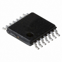
74LVC86APW,118 NXP Semiconductors, 74LVC86APW,118 Datasheet - Page 7

74LVC86APW,118
Manufacturer Part Number
74LVC86APW,118
Description
IC QUAD 2IN EXC-OR GATE 14TSSOP
Manufacturer
NXP Semiconductors
Series
74LVCr
Specifications of 74LVC86APW,118
Number Of Circuits
4
Package / Case
14-TSSOP
Logic Type
XOR (Exclusive OR)
Number Of Inputs
2
Current - Output High, Low
24mA, 24mA
Voltage - Supply
2.7 V ~ 3.6 V
Operating Temperature
-40°C ~ 125°C
Mounting Type
Surface Mount
Product
OR
Logic Family
LVC
High Level Output Current
- 24 mA
Low Level Output Current
24 mA
Propagation Delay Time
3 ns
Supply Voltage (max)
3.6 V
Supply Voltage (min)
1.2 V
Maximum Operating Temperature
+ 125 C
Mounting Style
SMD/SMT
Minimum Operating Temperature
- 40 C
Logical Function
XOR
Number Of Elements
4
Operating Supply Voltage (typ)
1.8/2.5/3.3V
Operating Temp Range
-40C to 125C
Package Type
TSSOP
Number Of Outputs
1
Technology
CMOS
Mounting
Surface Mount
Pin Count
14
Operating Temperature Classification
Automotive
Quiescent Current
40uA
Operating Supply Voltage (max)
3.6V
Operating Supply Voltage (min)
1.2V
Lead Free Status / RoHS Status
Lead free / RoHS Compliant
Lead Free Status / RoHS Status
Lead free / RoHS Compliant, Lead free / RoHS Compliant
Other names
74LVC86APW-T
74LVC86APW-T
935250110118
74LVC86APW-T
935250110118
Philips Semiconductors
Table 7:
Voltages are referenced to GND (ground = 0 V). For test circuit see
[1]
[2]
[3]
11. AC waveforms
74LVC86A_5
Product data sheet
Symbol
T
C
Fig 6. The inputs nA and nB to output nY propagation delay
amb
PD
Typical values are measured at T
Skew between any two outputs of the same package switching in the same direction. This parameter is guaranteed by design.
C
P
f
f
C
V
N = number of inputs switching,
Σ(C
i
o
D
CC
= 25 °C
PD
= input frequency in MHz,
L
= output frequency in MHz,
= output load capacitance in pF,
= C
L
is used to determine the dynamic power dissipation (P
= supply voltage in Volts,
× V
V
V
V
PD
M
M
OL
Parameter
power dissipation capacitance
per gate.
Dynamic characteristics
CC
= 1.5 V at V
= 0.5 × V
× V
and V
2
× f
CC
o
2
OH
) = sum of the outputs.
× f
CC
are typical output voltage drops that occur with the output load.
i
× N + Σ(C
CC
at V
≥ 2.7 V;
CC
< 2.7 V;
L
× V
amb
CC
nA, nB input
= 25 °C and V
nY output
2
…continued
× f
o
) where:
GND
V
V
Conditions
V
OH
OL
V
I
V
V
V
I
= GND to V
Rev. 05.00 — 15 May 2006
CC
CC
CC
CC
= 1.8 V, 2.5 V, 2.7 V, and 3.3 V respectively.
= 1.65 V to 1.95 V
= 2.3 V to 2.7 V
= 3.0 V to 3.6 V
D
in µW).
V
M
CC
V
M
t
PHL
Figure
7.
[3]
Min
-
-
-
t
PLH
mna224
Quad 2-input EXCLUSIVE-OR gate
© Koninklijke Philips Electronics N.V. 2006. All rights reserved.
Typ
13
16
20
[1]
74LVC86A
Max
-
-
-
Unit
pF
pF
pF
7 of 15


