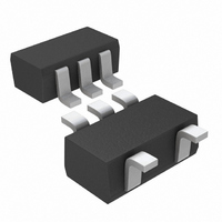
BU4S71G2-TR Rohm Semiconductor, BU4S71G2-TR Datasheet - Page 2

BU4S71G2-TR
Manufacturer Part Number
BU4S71G2-TR
Description
IC GATE OR SINGLE 5SSOP
Manufacturer
Rohm Semiconductor
Series
4Sr
Specifications of BU4S71G2-TR
Logic Type
OR Gate
Number Of Inputs
2
Number Of Circuits
1
Current - Output High, Low
3.4mA, 3.4mA
Voltage - Supply
3 V ~ 16 V
Operating Temperature
-40°C ~ 85°C
Mounting Type
Surface Mount
Package / Case
5-SSOP
Output Current
3.4mA
No. Of Inputs
2
Supply Voltage Range
3V To 16V
Logic Case Style
SSOP
No. Of Pins
5
Operating Temperature Range
-40°C To +85°C
Svhc
No SVHC (18-Jun-2010)
Lead Free Status / RoHS Status
Lead free / RoHS Compliant
Available stocks
Company
Part Number
Manufacturer
Quantity
Price
Part Number:
BU4S71G2-TR
Manufacturer:
ROHM/罗姆
Quantity:
20 000
●Absolute Maximum Ratings
●Recommended Operating Conditions
●Thermal Derating Curve
●Switching Characteristics
BU4S01G2,BU4S11G2,BU4SU69G2,BU4S71G2,BU4S81G2, BU4S584G2
© 2009 ROHM Co., Ltd. All rights reserved.
www.rohm.com
Power supply voltage
Supply current
Operating temperature
Storage temperature
Input voltage
Maximum junction temperature
Operating power supply
Input voltage
1400
1200
1000
800
600
400
200
Output
0
Input
0
Input
Output
25
Parameter
Parameter
10%
10%
10%
90%
20[ns]
20[ns]
①tpLH
50%
Ambient temperature Ta 〔℃〕
50
①tPHL
50%
③tTLH
50%
③tTHL
90%
90%
670[mV] BU4S Series (*1)
50%
90%
10%
75
20[ns]
20[ns]
85℃
②tPLH
④tTHL
100
④tTLH
②tpHL
BU4S01G2
BU4S11G2
BU4SU69G2
BU4S71G2
BU4S81G2
BU4S584G2
125
Symbol
Symbol
Tjmax
VDD
VDD
Topr
Tstg
VIN
VIN
Iin
150
BU4S01G2 BU4S11G2 BU4SU69G2 BU4S71G2 BU4S81G2 BU4S584G2
BU4S01G2 BU4S11G2 BU4SU69G2 BU4S71G2 BU4S81G2 BU4S584G2
175
Description of symbols
(1) tPHL: Time up to 50% of rise time of input waveform
(2) tPLH: Time up to 50% of fall time of input waveform
(3) tTHL: Time up to 90% ~ 10% of fall time of output waveform
(4) tTLH: Time up to 10% ~ 90% of rise time of output waveform
●Input / output Equivalent Circuits
Description of symbols
(1) tPLH: Time up to 50% of rise time of input waveform
(2) tPHL: Time up to 50% of fall time of input waveform
(3) tTLH: Time up to 10% ~ 90% of rise time of output waveform
(4) tTHL: Time up to 90% ~ 10% of fall time of output waveform
When used at Ta=25[°C] or above, values of above are reduced per 1[°C].
Power dissipation is the value for mounting 70[mm] x 70[mm] x 1.6[mm]
FR4 glass epoxy circuit board (copper foil area is 3% or less).
(*1)
5.3
2/16
~ 50% of fall time of output waveform
~ 50% of rise time of output waveform
~50% of rise time of output waveform
~ 50% of fall time of output waveform
VDD
GND
<
mW/℃
UNIT
Input
>
-0.3 to VDD+0.3
GND
VDD
-55 to 150
-0.3 to 18
0 to VDD
-40 to 85
3 to 16
Limit
Limit
±10
150
GND
VDD
<Output>
GND
VDD
Technical Note
2009.06 - Rev.A
Unit
Unit
mA
℃
℃
℃
V
V
V
V


