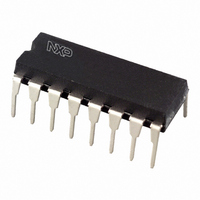
N74F166N,602 NXP Semiconductors, N74F166N,602 Datasheet - Page 7

N74F166N,602
Manufacturer Part Number
N74F166N,602
Description
IC SHIFT REGISTER 8BIT 16-DIP
Manufacturer
NXP Semiconductors
Series
74Fr
Datasheet
1.N74F166N602.pdf
(12 pages)
Specifications of N74F166N,602
Package / Case
16-DIP (0.300", 7.62mm)
Logic Type
Register, Bidirectional
Function
Universal
Output Type
Standard
Number Of Elements
1
Number Of Bits Per Element
8
Voltage - Supply
4.5 V ~ 5.5 V
Operating Temperature
-40°C ~ 85°C
Mounting Type
Through Hole
Counting Sequence
Serial/Parallel to Serial
Number Of Circuits
1
Logic Family
F
Propagation Delay Time
7.5 ns
Supply Voltage (max)
5.5 V
Maximum Operating Temperature
+ 70 C
Minimum Operating Temperature
0 C
Mounting Style
Through Hole
Supply Voltage (min)
4.5 V
Lead Free Status / RoHS Status
Lead free / RoHS Compliant
Lead Free Status / RoHS Status
Lead free / RoHS Compliant, Lead free / RoHS Compliant
Other names
568-3167-5
933794760602
N74F166N
933794760602
N74F166N
Philips Semiconductors
AC SETUP REQUIREMENTS
AC WAVEFORMS
Waveform 1. Propagation delay for clock input to output,
Feb. 14, 1991
SYMBOL
t
t
t
t
t
t
t
t
t
t
t
t
t
t
t
t
su
su
h
h
h
h
su
h
su
su
h
h
w
w
w
rec
8-bit bidirectional universal shift register
(H)
(L)
(H)
(L)
(H)
(H)
(L)
(L)
(L)
(L)
(L)
(L)
(H)
(H)
(H)
CP
Q7
clock pulse width, and maximum clock frequency
Setup time, high or low
Dn, Ds to CP, CE
Hold time, high or low
Dn, Ds to CP
Hold time, high or low
Dn, Ds to CE
Setup time, low
CE to CP
Hold time, high
CE to CP
Setup time, high or low
PE to CP, CE
Hold time, high or low
PE to CP
CP pulse width,
high or low
MR pulse width, low
Recovery time
V
t
PHL
M
PARAMETER
t
W
(H)
1/f
V
,
MAX
MR to CP
M
V
M
t
W
(L)
V
t
PLH
M
CONDITION
Waveform 3
Waveform 3
Waveform 3
Waveform 3
Waveform 3
Waveform 3
Waveform 3
Waveform 1
Waveform 2
Waveform 2
TEST
V
M
SF00287
MIN
3.0
2.5
0.0
0.0
1.5
0.0
5.0
0.0
3.0
3.0
0.0
0.0
3.0
4.5
4.0
4.0
T
V
amb
C
R
CC
L
L
7
TYP
= 50pF,
= 500
= +25 C
= +5.0V
Waveform 2. Master reset pulse width, master reset to output
Q7
MR
CP
MAX
V
CC
MIN
delay and master reset to clock recovery time
4.0
3.0
1.0
0.0
2.0
0.0
6.0
0.0
4.0
4.0
0.0
0.0
3.5
5.0
4.0
4.5
T
amb
C
R
= +5.0V
L
L
V
+70 C
t
PHL
= 50pF,
M
= 500
LIMITS
= 0 C to
t
w
(L)
MAX
V
10%
M
V
M
T
t
rec
amb
V
CC
MIN
4.0
3.0
1.0
0.0
2.0
0.0
6.0
0.0
4.0
6.0
0.0
0.0
3.5
6.0
4.0
4.5
= –40 C to +85 C
C
R
= +5.0V
V
L
L
M
= 50pF,
= 500
Product specification
74F166
MAX
10%
SF00288
SF00288
UNIT
ns
ns
ns
ns
ns
ns
ns
ns
ns
ns


