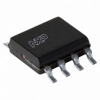
CBTD3306D,112 NXP Semiconductors, CBTD3306D,112 Datasheet - Page 7

CBTD3306D,112
Manufacturer Part Number
CBTD3306D,112
Description
IC FET BUS SWITCH 2BIT 8-SOIC
Manufacturer
NXP Semiconductors
Series
74CBTDr
Type
FET Bus Switchr
Datasheet
1.CBTD3306D112.pdf
(17 pages)
Specifications of CBTD3306D,112
Circuit
1 x 1:1
Independent Circuits
2
Current - Output High, Low
15mA, 64mA
Voltage Supply Source
Single Supply
Voltage - Supply
4.5 V ~ 5.5 V
Operating Temperature
-40°C ~ 85°C
Mounting Type
Surface Mount
Package / Case
8-SOIC (3.9mm Width)
Lead Free Status / RoHS Status
Lead free / RoHS Compliant
Other names
935270513112
CBTD3306D
CBTD3306D
CBTD3306D
CBTD3306D
NXP Semiconductors
11. Dynamic characteristics
Table 8.
Voltages are referenced to GND (ground = 0 V). For test circuit see
[1]
[2]
12. Waveforms
CBTD3306_4
Product data sheet
Symbol
t
t
t
pd
en
dis
Fig 11. The data input (nA, nB) to output (nB, nA) propagation delay times
The propagation delay is the calculated RC time constant of the typical ON resistance of the switch and the specified load capacitance,
when driven by an ideal voltage source (zero output impedance).
t
t
t
pd
en
dis
is the same as t
is the same as t
is the same as t
Measurement points are given in
Logic levels: V
Parameter
propagation delay
enable time
disable time
Dynamic characteristics
PLH
PZL
PLZ
OL
and t
and t
and t
and V
PZH
PHL
PHZ
OH
.
.
.
Conditions
nA, nB to nB, nA; see
nOE to nA or nB; see
nOE to nA or nB; see
are typical output voltage levels that occur with the output load.
V
V
V
CC
CC
CC
nA, nB
nB, nA
output
input
= 5.0 V ± 0.5 V
= 5.0 V ± 0.5 V
= 5.0 V ± 0.5 V
Table
GND
V
V
All information provided in this document is subject to legal disclaimers.
OH
OL
V
I
9.
Rev. 04 — 25 March 2010
V
Figure 12
Figure 12
M
Figure 11
V
M
t
PHL
Figure
13.
t
001aak305
PLH
[1][2]
[2]
[2]
Dual bus switch with level shifting
T
Min
1.0
1.0
amb
-
= −40 °C to +85 °C
Typ
CBTD3306
-
-
-
© NXP B.V. 2010. All rights reserved.
Max
0.25
5.4
4.9
Unit
ns
ns
ns
7 of 17


