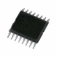
74LV251PW,112 NXP Semiconductors, 74LV251PW,112 Datasheet - Page 5

74LV251PW,112
Manufacturer Part Number
74LV251PW,112
Description
IC 8-INPUT MUX 3ST 16-TSSOP
Manufacturer
NXP Semiconductors
Series
74LVr
Type
Multiplexerr
Datasheet
1.74LV251N112.pdf
(12 pages)
Specifications of 74LV251PW,112
Package / Case
16-TSSOP
Circuit
1 x 8:1
Independent Circuits
1
Current - Output High, Low
6mA, 6mA
Voltage Supply Source
Single Supply
Voltage - Supply
1 V ~ 3.6 V
Operating Temperature
-40°C ~ 125°C
Mounting Type
Surface Mount
Product
Decoders, Encoders, Multiplexers & Demultiplexers
Logic Family
74LV
Number Of Bits
8
Number Of Lines (input / Output)
9.0 / 2.0
Propagation Delay Time
20 ns
Supply Voltage (max)
3.6 V
Supply Voltage (min)
1 V
Maximum Operating Temperature
+ 125 C
Minimum Operating Temperature
- 40 C
Mounting Style
SMD/SMT
Number Of Input Lines
9.0
Number Of Output Lines
2.0
Power Dissipation
500 mW
Lead Free Status / RoHS Status
Lead free / RoHS Compliant
Lead Free Status / RoHS Status
Lead free / RoHS Compliant, Lead free / RoHS Compliant
Other names
568-2946-5
935174670112
935174670112
1. Stresses beyond those listed may cause permanent damage to the device. These are stress ratings only and functional operation of the
2. The input and output voltage ratings may be exceeded if the input and output current ratings are observed.
Philips Semiconductors
ABSOLUTE MAXIMUM RATINGS
In accordance with the Absolute Maximum Rating System (IEC 134).
Voltages are referenced to GND (ground = 0 V).
NOTES:
DC ELECTRICAL CHARACTERISTICS
Over recommended operating conditions. Voltages are referenced to GND (ground = 0 V).
1998 May 20
SYMBOL
SYMBOL
8-input multiplexer (3-State)
"I
device at these or any other conditions beyond those indicated under “recommended operating conditions” is not implied. Exposure to
absolute-maximum-rated conditions for extended periods may affect device reliability.
V
V
V
"I
"I
V
V
V
P
V
"I
V
"I
V
T
O
OH
OH
O
OL
OL
TOT
GND
IH
stg
IL
CC
OK
CC
IK
O
,
HIGH level Input
voltage
voltage
LOW level Input
voltage
voltage
HIGH level output
voltage; all outputs
HIGH level output
voltage;
STANDARD
outputs
LOW level output
voltage; all outputs
LOW level output
voltage;
STANDARD
outputs
DC supply voltage
DC input diode current
DC output diode current
DC output source or sink current
– standard outputs
DC V
– standard outputs
Storage temperature range
Power dissipation per package
– plastic DIL
– plastic mini-pack (SO)
– plastic shrink mini-pack (SSOP and TSSOP)
PARAMETER
CC
or GND current for types with
PARAMETER
V
V
V
V
V
V
V
V
V
V
V
V
V
V
V
V
CC
CC
CC
CC
CC
CC
CC
CC
CC
CC
CC
CC
CC
CC
CC
CC
= 1.2 V
= 2.0 V
= 2.7 to 3.6 V
= 1.2 V
= 2.0 V
= 2.7 to 3.6 V
= 1.2 V; V
= 2.0 V; V
= 2.7 V; V
= 3.0 V; V
= 3.0 V; V
= 1.2 V; V
= 2.0 V; V
= 2.7 V; V
= 3.0 V; V
= 3.0 V; V
1, 2
TEST CONDITIONS
I
I
I
I
I
I
I
I
I
I
= V
= V
= V
= V
= V
= V
= V
= V
= V
= V
IH
IH
IH
IH
IH
IH
IH
IH
IH
IH
or V
or V
or V
or V
or V
or V
or V
or V
or V
or V
IL;
IL;
IL;
IL;
IL;
IL;
IL;
IL;
IL;
IL;
–I
–I
–I
–I
–I
I
I
I
I
I
O
O
O
O
O
V
V
–0.5V < V
for temperature range: –40 to +125 C
above +70 C derate linearly with 12 mW/K
above +70 C derate linearly with 8 mW/K
above +60 C derate linearly with 5.5 mW/K
O
O
O
O
O
= 100 A
= 100 A
= 100 A
= 100 A
= 6mA
I
O
= 100 A
= 100 A
= 100 A
= 100 A
= 6mA
< –0.5 or V
< –0.5 or V
5
O
< V
I
O
> V
CONDITIONS
CC
> V
2.40
MIN
0.9
1.4
2.0
1.8
2.5
2.8
CC
+ 0.5V
CC
+ 0.5V
-40 C to +85 C
+ 0.5V
TYP
2.82
0.25
1.2
2.0
2.7
3.0
0
0
0
0
1
MAX
LIMITS
0.40
0.3
0.6
0.8
0.2
0.2
0.2
2.20
–0.5 to +4.6
–65 to +150
-40 C to +125 C
MIN
0.9
1.4
2.0
1.8
2.5
2.8
RATING
750
500
400
20
50
25
50
Product specification
74LV251
MAX
0.50
0.3
0.6
0.8
0.2
0.2
0.2
UNIT
mW
mA
mA
mA
mA
V
UNIT
C
V
V
V
V
V
V
V
V


