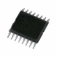
74LV251PW,112 NXP Semiconductors, 74LV251PW,112 Datasheet - Page 7

74LV251PW,112
Manufacturer Part Number
74LV251PW,112
Description
IC 8-INPUT MUX 3ST 16-TSSOP
Manufacturer
NXP Semiconductors
Series
74LVr
Type
Multiplexerr
Datasheet
1.74LV251N112.pdf
(12 pages)
Specifications of 74LV251PW,112
Package / Case
16-TSSOP
Circuit
1 x 8:1
Independent Circuits
1
Current - Output High, Low
6mA, 6mA
Voltage Supply Source
Single Supply
Voltage - Supply
1 V ~ 3.6 V
Operating Temperature
-40°C ~ 125°C
Mounting Type
Surface Mount
Product
Decoders, Encoders, Multiplexers & Demultiplexers
Logic Family
74LV
Number Of Bits
8
Number Of Lines (input / Output)
9.0 / 2.0
Propagation Delay Time
20 ns
Supply Voltage (max)
3.6 V
Supply Voltage (min)
1 V
Maximum Operating Temperature
+ 125 C
Minimum Operating Temperature
- 40 C
Mounting Style
SMD/SMT
Number Of Input Lines
9.0
Number Of Output Lines
2.0
Power Dissipation
500 mW
Lead Free Status / RoHS Status
Lead free / RoHS Compliant
Lead Free Status / RoHS Status
Lead free / RoHS Compliant, Lead free / RoHS Compliant
Other names
568-2946-5
935174670112
935174670112
Philips Semiconductors
AC WAVEFORMS
V
V
V
output load.
V
V
V
V
1998 May 20
M
M
OL
X
X
Y
Y
8-input multiplexer (3-State)
= V
= V
= V
= V
Figure 2. Multiplexer input (I
= 1.5 V at V
= 0.5 V
and V
Figure 1. Multiplexer input (I
I n , S n INPUT
OL
OL
OH
OH
I
Y OUTPUT
n
+ 0.3 V at V
+ 0.1 V
, S
Y OUTPUT
OH
– 0.3 V at V
– 0.1
n
V
V OH
are the typical output voltage drop that occur with the
V CC
GND
INPUT
V OL
CC
V CC
GND
V OH
V OL
CC
at V
V
output (Y) propagation delays.
output (Y) propagation delays.
CC
CC
t PHL
t PHL
2.7 V
CC
at V
CC
CC
at V
CC
2.7 V
2.7 V
CC
2.7V
V M
V M
2.7 V
2.7 V
V M
V M
n)
n
and the select input (S
) and select input (S
SV00633
SV00634
t PLH
t PLH
n
) to
n
) to
7
TEST CIRCUIT
HIGH-to-OFF
OFF-to-HIGH
GENERATOR
LOW-to-OFF
OFF-to-LOW
DEFINITIONS
C
OE INPUT
R
R
PULSE
OUTPUT
OUTPUT
L
T
L
= Load capacitance includes jig and probe capacitance
= Termination resistance should be equal to Z
= Load resistor
Figure 4. Load circuitry for switching times.
GND
V OH
GND
V CC
V CC
V OL
Figure 3. 3-State enable and disable times
t
PLH/
TEST
t
PHL
Test Circuit for switching times
enabled
outputs
V
I
V M
R
t PLZ
t PHZ
T
V X
D.U.T.
V
V Y
CC
2.7–3.6V
< 2.7V
V
CC
disabled
outputs
V
O
C
OUT
L
2.7V
V
V
CC
of pulse generators.
t PZL
I
Product specification
t PZH
50pF
74LV251
V M
SV00776
V M
R
L
SV00635
= 1K
enabled
outputs


