SSTUA32864EC/G,518 NXP Semiconductors, SSTUA32864EC/G,518 Datasheet - Page 10
SSTUA32864EC/G,518
Manufacturer Part Number
SSTUA32864EC/G,518
Description
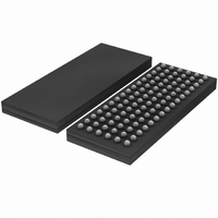
IC REG BUFFER 25BIT 96-LFBGA
Manufacturer
NXP Semiconductors
Datasheet
1.SSTUA32864ECG518.pdf
(20 pages)
Specifications of SSTUA32864EC/G,518
Logic Type
1:1, 1:2 Configurable Registered Buffer
Supply Voltage
1.7 V ~ 2 V
Number Of Bits
25, 14
Operating Temperature
0°C ~ 70°C
Mounting Type
Surface Mount
Package / Case
96-LFBGA
Logic Family
SSTU
Logical Function
Registered Buffer
Number Of Elements
1
Number Of Inputs
25
Number Of Outputs
25
High Level Output Current
-8mA
Low Level Output Current
8mA
Package Type
LFBGA
Propagation Delay Time
3ns
Operating Supply Voltage (typ)
1.8V
Operating Supply Voltage (max)
2V
Operating Supply Voltage (min)
1.7V
Clock-edge Trigger Type
Posit/Negat-Edge
Polarity
Non-Inverting
Technology
CMOS
Frequency (max)
450(Min)MHz
Mounting
Surface Mount
Pin Count
96
Operating Temp Range
0C to 70C
Operating Temperature Classification
Commercial
Lead Free Status / RoHS Status
Lead free / RoHS Compliant
Other names
568-3538-2
935279443518
SSTUA32864EC/G-T
935279443518
SSTUA32864EC/G-T
Available stocks
Company
Part Number
Manufacturer
Quantity
Price
Company:

Part Number:
SSTUA32864EC/G,518
Manufacturer:
NXP Semiconductors
Quantity:
10 000


NXP Semiconductors
Table 7.
Recommended operating conditions; T
See
[1]
[2]
[3]
Table 8.
Recommended operating conditions; T
Class I, V
[1]
[2]
Table 9.
Recommended operating conditions; V
SSTUA32864_2
Product data sheet
Symbol
f
t
t
t
t
t
Symbol
f
t
t
t
Symbol
dV/dt_r
dV/dt_f
dV/dt_
clock
W
ACT
INACT
su
h
max
PDM
PDMSS
PHL
This parameter is not necessarily production tested.
Data inputs must be active below a minimum time of t
Data and clock inputs must be held at valid levels (not floating) a minimum time of t
Includes 350 ps of test-load transmission line delay.
This parameter is not necessarily production tested.
Figure 6
ref
Timing requirements
Switching characteristics
Output edge rates
= V
Parameter
clock frequency
pulse width
differential inputs active time
differential inputs inactive time
set-up time
hold time
through
Parameter
maximum input clock frequency
peak propagation delay
simultaneous switching peak
propagation delay
HIGH-to-LOW propagation delay
Parameter
rising edge slew rate
falling edge slew rate
absolute difference between dV/dt_r
and dV/dt_f
T
= V
DD
Figure
0.5 and C
11.
L
= 10 pF; unless otherwise specified. See
amb
amb
DD
1.8 V configurable registered buffer for DDR2-667 RDIMM applications
= 1.8 V
= 0 C to +70 C; V
= 0 C to +70 C; V
Conditions
CK, CK HIGH or LOW
DCS before CK , CK , CSR HIGH
DCS before CK , CK , CSR LOW
CSR, ODT, CKE, and data before
CK , CK
DCS, CSR, ODT, CKE, and data
after CK , CK
Rev. 02 — 9 March 2007
Conditions
CK and CK to output
CK and CK to output
RESET to output
0.1 V; unless otherwise specified.
Conditions
ACT(max)
after RESET is taken HIGH.
DD
DD
= 1.8 V
= 1.8 V
0.1 V; unless otherwise specified.
0.1 V;
INACT(max)
Figure 6
[1][2]
[1]
[1][2]
[1][3]
after RESET is taken LOW.
Min
450
1.2
-
-
Min
1
1
-
through
Min
-
1
-
-
0.7
0.5
0.5
0.5
SSTUA32864
Figure
Typ
-
-
-
-
Typ
-
-
-
Typ
-
-
-
-
-
-
-
-
11.
© NXP B.V. 2007. All rights reserved.
Max
-
1.8
2.0
3
Max
4
4
1
Max
450
-
10
15
-
-
-
-
Unit
MHz
ns
ns
ns
Unit
V/ns
V/ns
V/ns
Unit
MHz
ns
ns
ns
ns
ns
ns
ns
10 of 20
Related parts for SSTUA32864EC/G,518
Image
Part Number
Description
Manufacturer
Datasheet
Request
R

Part Number:
Description:
NXP Semiconductors designed the LPC2420/2460 microcontroller around a 16-bit/32-bitARM7TDMI-S CPU core with real-time debug interfaces that include both JTAG andembedded trace
Manufacturer:
NXP Semiconductors
Datasheet:

Part Number:
Description:
NXP Semiconductors designed the LPC2458 microcontroller around a 16-bit/32-bitARM7TDMI-S CPU core with real-time debug interfaces that include both JTAG andembedded trace
Manufacturer:
NXP Semiconductors
Datasheet:
Part Number:
Description:
NXP Semiconductors designed the LPC2468 microcontroller around a 16-bit/32-bitARM7TDMI-S CPU core with real-time debug interfaces that include both JTAG andembedded trace
Manufacturer:
NXP Semiconductors
Datasheet:
Part Number:
Description:
NXP Semiconductors designed the LPC2470 microcontroller, powered by theARM7TDMI-S core, to be a highly integrated microcontroller for a wide range ofapplications that require advanced communications and high quality graphic displays
Manufacturer:
NXP Semiconductors
Datasheet:
Part Number:
Description:
NXP Semiconductors designed the LPC2478 microcontroller, powered by theARM7TDMI-S core, to be a highly integrated microcontroller for a wide range ofapplications that require advanced communications and high quality graphic displays
Manufacturer:
NXP Semiconductors
Datasheet:
Part Number:
Description:
The Philips Semiconductors XA (eXtended Architecture) family of 16-bit single-chip microcontrollers is powerful enough to easily handle the requirements of high performance embedded applications, yet inexpensive enough to compete in the market for hi
Manufacturer:
NXP Semiconductors
Datasheet:
Part Number:
Description:
The XA-S3 device is a member of Philips Semiconductors? XA(eXtended Architecture) family of high performance 16-bitsingle-chip microcontrollers
Manufacturer:
NXP Semiconductors
Datasheet:

Part Number:
Description:
The NXP BlueStreak LH75401/LH75411 family consists of two low-cost 16/32-bit System-on-Chip (SoC) devices
Manufacturer:
NXP Semiconductors
Datasheet:
Part Number:
Description:
The NXP LPC3130/3131 combine an 180 MHz ARM926EJ-S CPU core, high-speed USB2
Manufacturer:
NXP Semiconductors
Datasheet:
Part Number:
Description:
The NXP LPC3141 combine a 270 MHz ARM926EJ-S CPU core, High-speed USB 2
Manufacturer:
NXP Semiconductors
Part Number:
Description:
The NXP LPC3143 combine a 270 MHz ARM926EJ-S CPU core, High-speed USB 2
Manufacturer:
NXP Semiconductors

Part Number:
Description:
The NXP LPC3152 combines an 180 MHz ARM926EJ-S CPU core, High-speed USB 2
Manufacturer:
NXP Semiconductors
Part Number:
Description:
The NXP LPC3154 combines an 180 MHz ARM926EJ-S CPU core, High-speed USB 2
Manufacturer:
NXP Semiconductors

Part Number:
Description:
Standard level N-channel enhancement mode Field-Effect Transistor (FET) in a plastic package using NXP High-Performance Automotive (HPA) TrenchMOS technology
Manufacturer:
NXP Semiconductors
Datasheet: