SSTUB32868ET/G,518 NXP Semiconductors, SSTUB32868ET/G,518 Datasheet
SSTUB32868ET/G,518
Specifications of SSTUB32868ET/G,518
Available stocks


Related parts for SSTUB32868ET/G,518


SSTUB32868ET/G,518 Summary of contents
Page 1
SSTUB32868 1.8 V 28-bit configurable registered buffer with parity for DDR2-800 RDIMM applications Rev. 04 — 22 April 2010 1. General description The SSTUB32868 is a 1.8 V 28-bit register specifically designed for use ...
Page 2
... NXP Semiconductors Two additional chip select inputs allow optional flexible enabling and disabling Supports Stub Series Terminated Logic SSTL_18 data inputs Differential clock (CK and CK) inputs Supports Low Voltage Complementary Metal-Oxide Semiconductor (LVCMOS) switching levels on the control and RESET inputs Single 1.8 V supply operation (1 2.0 V) Available in 176-ball 6 mm × ...
Page 3
... NXP Semiconductors 5. Functional diagram RESET VREF DCKE0, DCKE1 DODT0, DODT1 DCS0 CSGEN DCS1 DCS2 DCS3 (1) Register A configuration ( D5, D7 D12, D17 to D28 Fig 1. SSTUB32868_4 Product data sheet 1.8 V DDR2-800 configurable registered buffer with parity SSTUB32868 ( other channels Register B configuration ( D12, D17 to D20, D22, D24 to D28 Logic diagram of SSTUB32868 (positive logic) All information provided in this document is subject to legal disclaimers ...
Page 4
... NXP Semiconductors RESET CK CK (1) Dn VREF PAR_IN DCS0 CSGEN DCS1 DCS2 DCS3 (1) Register A configuration ( D5, D7 D12, D17 to D28 (2) Register A configuration (C = 0): Q1A to Q5A, Q7A, Q9A to Q12A, Q17A to Q28A (3) Register A configuration (C = 0): Q1B to Q5B, Q7B, Q9B to Q12B, Q17B to Q28B Fig 2. SSTUB32868_4 Product data sheet 1 ...
Page 5
... NXP Semiconductors 6. Pinning information 6.1 Pinning Fig 3. SSTUB32868_4 Product data sheet 1.8 V DDR2-800 configurable registered buffer with parity ball A1 index area Pin configuration for TFBGA176 All information provided in this document is subject to legal disclaimers. Rev. 04 — 22 April 2010 SSTUB32868 SSTUB32868ET/G SSTUB32868ET 002aac337 Transparent top view © ...
Page 6
... NXP Semiconductors Fig 4. SSTUB32868_4 Product data sheet 1.8 V DDR2-800 configurable registered buffer with parity GND (DCKE1 (DCKE0) Q6A D9 GND (QCKE1A) Q8A D10 V DD (QCKE0A) D11 Q10A GND D12 Q12A V DD DCS1 QCS1A GND (D13) (Q13A) DCS0 QCS0A DCS2 (D14) (Q14A) CK CSGEN ...
Page 7
... NXP Semiconductors Fig 5. SSTUB32868_4 Product data sheet 1.8 V DDR2-800 configurable registered buffer with parity GND Q6A GND D10 Q8A V DD D11 Q10A GND D12 Q12A V DD D13 Q13A GND (DODT1) (QODT1A) D14 Q14A DCS2 (DODT0) (QODT0A) CK CSGEN PAR_IN CK RESET QERR D15 ...
Page 8
... NXP Semiconductors 6.2 Pin description Table 3. Pin description Symbol Pin Register Ungated inputs DCKE0 D1 DCKE1 C1 DODT0 N1 DODT1 P1 Chip Select gated inputs D1 to A2, A1, B2, B1, C2, C1, D28 D2, D1, E1, F1, G1, H1, N1, P1, R1, T1, U1, V1, W1, W2, Y1, Y2, AA1, AA2, AB1, AB2 Chip Select inputs ...
Page 9
... NXP Semiconductors Table 3. Pin description …continued Symbol Pin Register QODT0A N2 QODT0B M7 QODT1A P2 QODT1B M8 Output error QERR M3 Parity input PAR_IN L3 Program inputs CSGEN L2 Clock inputs Miscellaneous inputs RESET M2 VREF A5, AB5 V B3, B4, B5, B6, D3, D4, DD D5, D6, F3, F4, F5, F6, H3, H4, H5, H6, K4, K5, K6, M4, M5, M6, P4, P5, ...
Page 10
... NXP Semiconductors [1] Data inputs = D1 to D5, D7 D12, D17 to D28 when Data inputs = D1 to D12, D17 to D20, D22, D24 to D28 when [2] Data outputs = Q1x to Q5x, Q7x, Q9x to Q12x, Q17x to Q28x when Data outputs = Q1x to Q12x, Q17x to Q20x, Q22x, Q24x to Q28x when Functional description 7 ...
Page 11
... NXP Semiconductors Table 5. Parity and standby function table [1] RESET DCS0 DCS1 floating X or floating [1] DCS2 and DCS3 operate identically to DCS0 and DCS1 with regard to the parity function. [2] PAR_IN arrives one clock cycle after the data to which it applies. [3] This transition assumes QERR is HIGH at the crossing of CK going HIGH and CK going LOW. If QERR is LOW, it stays latched LOW for two clock cycles or until RESET is driven LOW ...
Page 12
... NXP Semiconductors during the time from the LOW-to-HIGH transition of RESET until the input receivers are fully enabled, the design of the SSTUB32868 must ensure that the outputs will remain LOW, thus ensuring no glitches on the output. The SSTUB32868 includes a parity checking function. Parity, which arrives one cycle after the data input to which it applies, is checked on the PAR_IN input of the device ...
Page 13
... NXP Semiconductors 7.3 Register timing RESET CSGEN DCSn CK CK Dn, DODTn, (1) DCKEn Qn, QODTn, QCKEn (1) PAR_IN (2) QERR HIGH, LOW, or Don't care (1) After RESET is switched from LOW to HIGH, all data and PAR_IN input signals must be set and held LOW for a minimum time avoid false error. ...
Page 14
... NXP Semiconductors RESET CSGEN DCSn CK CK Dn, DODTn, DCKEn Qn, QODTn, QCKEn PAR_IN (1) QERR unknown input event (1) If the data is clocked in on the m clock pulse, and PAR_IN is clocked the QERR output signal will be generated on the clock pulse and it will be valid on the clock pulse error occurs and the QERR output is driven LOW, it stays LOW for a minimum of two clock cycles or until RESET is driven LOW ...
Page 15
... NXP Semiconductors RESET (1) CSGEN (1) DCSn (1) CK (1) CK Dn, DODTn, (1) DCKEn Qn, QODTn, QCKEn (1) PAR_IN QERR (1) After RESET is switched from HIGH to LOW, all data and clock input signals must be held at valid logic levels (not floating) for a minimum time of t INACT(max) Fig 8. Timing diagram during shutdown (RESET switches from HIGH to LOW) ...
Page 16
... NXP Semiconductors 8. Limiting values Table 6. Limiting values In accordance with the Absolute Maximum Rating System (IEC 60134). Symbol Parameter V supply voltage DD V input voltage I V output voltage O I input clamping current IK I output clamping current OK I output current O I continuous current through ...
Page 17
... NXP Semiconductors 10. Characteristics Table 8. Characteristics Over recommended operating conditions, unless otherwise noted. Symbol Parameter V HIGH-level output voltage LOW-level output voltage input current I I supply current DD I dynamic operating current DDD per MHz C input capacitance i Z output impedance o Input RESET V LOW-level input voltage ...
Page 18
... NXP Semiconductors Table 9. Timing requirements Over recommended operating conditions, unless otherwise noted. Symbol Parameter f clock frequency clk t pulse width W t differential inputs active time ACT t differential inputs inactive INACT time t set-up time su t hold time h [1] This parameter is not necessarily production tested. ...
Page 19
... NXP Semiconductors 11. Test information 11.1 Parameter measurement information for data output load circuit = 1.8 V ± 0 All input pulses are supplied by generators having the following characteristics: Pulse Repetition Rate (PRR) ≤ 10 MHz; Z unless otherwise specified. The outputs are measured one at a time with one transition per measurement. ...
Page 20
... NXP Semiconductors Fig 12. Voltage waveforms; setup and hold times Fig 13. Voltage waveforms; propagation delay times (clock to output) Fig 14. Voltage waveforms; propagation delay times (reset to output) SSTUB32868_4 Product data sheet 1.8 V DDR2-800 configurable registered buffer with parity input V ref V = 600 mV 0.5V . ref ...
Page 21
... NXP Semiconductors 11.2 Data output slew rate measurement = 1.8 V ± 0 All input pulses are supplied by generators having the following characteristics: PRR ≤ 10 MHz; Z (1) C Fig 15. Load circuit, HIGH-to-LOW slew measurement Fig 16. Voltage waveforms, HIGH-to-LOW slew rate measurement (1) C Fig 17. Load circuit, LOW-to-HIGH slew measurement Fig 18 ...
Page 22
... NXP Semiconductors 11.3 Error output load circuit and voltage measurement = 1.8 V ± 0 All input pulses are supplied by generators having the following characteristics: PRR ≤ 10 MHz; Z (1) C Fig 19. Load circuit, error output measurements Fig 20. Voltage waveforms, open-drain output LOW-to-HIGH transition time with respect Fig 21 ...
Page 23
... NXP Semiconductors Fig 22. Voltage waveforms, open-drain output LOW-to-HIGH transition time with respect SSTUB32868_4 Product data sheet 1.8 V DDR2-800 configurable registered buffer with parity timing V ICR inputs t PLH output waveform 2 to clock inputs All information provided in this document is subject to legal disclaimers. Rev. 04 — 22 April 2010 ...
Page 24
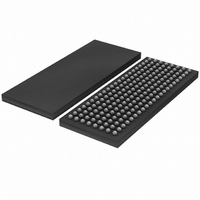
... NXP Semiconductors 12. Package outline TFBGA176: plastic thin fine-pitch ball grid array package; 176 balls; body 0.7 mm ball A1 index area ball A1 index area DIMENSIONS (mm are the original dimensions) A UNIT max 0.35 0.80 0.45 mm 1.15 0.25 0.65 0.35 OUTLINE VERSION IEC SOT932 Fig 23. Package outline SOT932-1 (TFBGA176) ...
Page 25
... NXP Semiconductors 13. Soldering of SMD packages This text provides a very brief insight into a complex technology. A more in-depth account of soldering ICs can be found in Application Note AN10365 “Surface mount reflow soldering description”. 13.1 Introduction to soldering Soldering is one of the most common methods through which packages are attached to Printed Circuit Boards (PCBs), to form electrical circuits ...
Page 26
... NXP Semiconductors 13.4 Reflow soldering Key characteristics in reflow soldering are: • Lead-free versus SnPb soldering; note that a lead-free reflow process usually leads to higher minimum peak temperatures (see reducing the process window • Solder paste printing issues including smearing, release, and adjusting the process window for a mix of large and small components on one board • ...
Page 27
... NXP Semiconductors Fig 24. Temperature profiles for large and small components For further information on temperature profiles, refer to Application Note AN10365 “Surface mount reflow soldering description”. 14. Abbreviations Table 14. Acronym CMOS DDR2 DIMM DRAM LVCMOS RDIMM SSTL 15. Revision history Table 15. Revision history Document ID ...
Page 28
... Terms and conditions of commercial sale of NXP Semiconductors. Right to make changes — NXP Semiconductors reserves the right to make changes to information published in this document, including without limitation specifications and product descriptions, at any time and without notice ...
Page 29
... NXP Semiconductors’ specifications such use shall be solely at customer’s own risk, and (c) customer fully indemnifies NXP Semiconductors for any liability, damages or failed product claims resulting from customer design and use of the product for automotive applications beyond NXP Semiconductors’ ...
Page 30
... NXP Semiconductors 18. Contents 1 General description . . . . . . . . . . . . . . . . . . . . . . 1 2 Features and benefits . . . . . . . . . . . . . . . . . . . . 1 3 Applications . . . . . . . . . . . . . . . . . . . . . . . . . . . . 2 4 Ordering information . . . . . . . . . . . . . . . . . . . . . 2 4.1 Ordering options . . . . . . . . . . . . . . . . . . . . . . . . 2 5 Functional diagram . . . . . . . . . . . . . . . . . . . . . . 3 6 Pinning information . . . . . . . . . . . . . . . . . . . . . . 5 6.1 Pinning . . . . . . . . . . . . . . . . . . . . . . . . . . . . . . . 5 6.2 Pin description . . . . . . . . . . . . . . . . . . . . . . . . . 8 7 Functional description . . . . . . . . . . . . . . . . . . 10 7.1 Function table . . . . . . . . . . . . . . . . . . . . . . . . . 10 7.2 Functional information . . . . . . . . . . . . . . . . . . 11 7.3 Register timing . . . . . . . . . . . . . . . . . . . . . . . . 13 8 Limiting values Recommended operating conditions ...