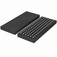
SSTUA32866EC/G,551 NXP Semiconductors, SSTUA32866EC/G,551 Datasheet - Page 7

SSTUA32866EC/G,551
Manufacturer Part Number
SSTUA32866EC/G,551
Description
IC BUFFER 1.8V 25BIT SOT536-1
Manufacturer
NXP Semiconductors
Datasheet
1.SSTUA32866ECG518.pdf
(28 pages)
Specifications of SSTUA32866EC/G,551
Logic Type
1:1, 1:2 Configurable Registered Buffer with Parity
Supply Voltage
1.7 V ~ 2 V
Number Of Bits
25, 14
Operating Temperature
0°C ~ 70°C
Mounting Type
Surface Mount
Package / Case
96-LFBGA
Lead Free Status / RoHS Status
Lead free / RoHS Compliant
Other names
935279442551
SSTUA32866EC/G-S
SSTUA32866EC/G-S
SSTUA32866EC/G-S
SSTUA32866EC/G-S
NXP Semiconductors
7. Functional description
SSTUA32866_2
Product data sheet
Table 2.
[1]
[2]
[3]
The SSTUA32866 is a 25-bit 1 : 1 or 14-bit 1 : 2 configurable registered buffer with parity,
designed for 1.7 V to 2.0 V V
All clock and data inputs are compatible with the JEDEC standard for SSTL_18. The
control and reset (RESET) inputs are LVCMOS. All data outputs are 1.8 V CMOS drivers
that have been optimized to drive the DDR2 DIMM load, and meet SSTL_18
specifications. The error (QERR) output is 1.8 V open-drain driver.
The SSTUA32866 operates from a differential clock (CK and CK). Data are registered at
the crossing of CK going HIGH, and CK going LOW.
The C0 input controls the pinout configuration for the 1 : 2 pinout from A configuration
(when LOW) to B configuration (when HIGH). The C1 input controls the pinout
configuration from 25-bit 1 : 1 (when LOW) to 14-bit 1 : 2 (when HIGH).
The SSTUA32866 accepts a parity bit from the memory controller on its parity bit
(PAR_IN) input, compares it with the data received on the DIMM-independent D-inputs
and indicates whether a parity error has occurred on its open-drain QERR pin
(active LOW). The convention is even parity, that is, valid parity is defined as an even
number of ones across the DIMM-independent data inputs combined with the parity input
bit.
When used as a single device, the C0 and C1 inputs are tied LOW. In this configuration,
parity is checked on the PAR_IN input which arrives one cycle after the input data to which
it applies. The Partial-Parity-Out (PPO) and QERR signals are produced three cycles after
the corresponding data inputs.
When used in pairs, the C0 input of the first register is tied LOW and the C0 input of the
second register is tied HIGH. The C1 input of both registers are tied HIGH. Parity, which
arrives one cycle after the data input to which it applies, is checked on the PAR_IN input of
the first device. The PPO and QERR signals are produced on the second device three
clock cycles after the corresponding data inputs. The PPO output of the first register is
Symbol
QERR
n.c.
DNU
Depends on configuration. See
Data inputs = D2, D3, D5, D6, D8 to D25 when C0 = 0 and C1 = 0.
Data inputs = D2, D3, D5, D6, D8 to D14 when C0 = 0 and C1 = 1.
Data inputs = D1 to D6, D8 to D10, D12, D13 when C0 = 1 and C1 = 1.
Data outputs = Q2, Q3, Q5, Q6, Q8 to Q25 when C0 = 0 and C1 = 0.
Data outputs = Q2, Q3, Q5, Q6, Q8 to Q14 when C0 = 0 and C1 = 1.
Data outputs = Q1 to Q6, Q8 to Q10, Q12, Q13 when C0 = 1 and C1 = 1.
Pin description
Pin
D2
[1]
[1]
Rev. 02 — 26 March 2007
…continued
1.8 V DDR2-667 configurable registered buffer with parity
DD
Figure
operation.
Type
open-drain
output
-
-
4,
Figure
5, and
Figure 6
Description
Output error bit (active LOW). Generated
one clock cycle after the corresponding
data output
Not connected. Ball present but no
internal connection to the die.
Do not use. Inputs are in
standby-equivalent mode and outputs
are driven LOW.
for ball number.
SSTUA32866
© NXP B.V. 2007. All rights reserved.
7 of 28


