74AUP1T98GW,125 NXP Semiconductors, 74AUP1T98GW,125 Datasheet - Page 13
74AUP1T98GW,125
Manufacturer Part Number
74AUP1T98GW,125
Description
IC LP CONFIG GATE V-XLATR UMT6
Manufacturer
NXP Semiconductors
Series
74AUPr
Datasheet
1.74AUP1T98GW125.pdf
(20 pages)
Specifications of 74AUP1T98GW,125
Package / Case
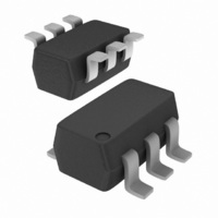
SC-70-6, SC-88, SOT-363
Logic Function
Translator
Number Of Bits
3
Input Type
Voltage
Output Type
Voltage
Number Of Channels
3
Number Of Outputs/channel
1
Differential - Input:output
No/No
Propagation Delay (max)
3.8ns
Voltage - Supply
2.3 V ~ 3.6 V
Operating Temperature
-40°C ~ 125°C
Supply Voltage
2.3 V ~ 3.6 V
Logic Family
74AUP
Translation
CMOS to CMOS
Propagation Delay Time
6.8 ns
Supply Voltage (max)
3.6 V
Supply Voltage (min)
2.3 V
Maximum Operating Temperature
+ 125 C
Minimum Operating Temperature
- 40 C
Maximum Power Dissipation
250 mW
Mounting Style
SMD/SMT
Lead Free Status / RoHS Status
Lead free / RoHS Compliant
Data Rate
-
Lead Free Status / Rohs Status
Lead free / RoHS Compliant
Other names
568-4753-2
74AUP1T98GW,125
74AUP1T98GW-G
74AUP1T98GW-G
935280471125
74AUP1T98GW,125
74AUP1T98GW-G
74AUP1T98GW-G
935280471125


NXP Semiconductors
Fig 15. Package outline SOT886 (XSON6)
74AUP1T98
Product data sheet
XSON6: plastic extremely thin small outline package; no leads; 6 terminals; body 1 x 1.45 x 0.5 mm
DIMENSIONS (mm are the original dimensions)
Notes
1. Including plating thickness.
2. Can be visible in some manufacturing processes.
UNIT
mm
VERSION
OUTLINE
SOT886
max
A
0.5
(1)
max
0.04
A
terminal 1
index area
1
e
0.25
0.17
b
6×
(2)
L
1
IEC
1.5
1.4
D
1.05
0.95
1
6
E
0
e
MO-252
JEDEC
1
0.6
All information provided in this document is subject to legal disclaimers.
e
REFERENCES
D
0.5
2
5
e
1
Rev. 2 — 19 October 2010
e
0.35
0.27
1
L
Low-power configurable gate with voltage-level translator
JEITA
b
0.40
0.32
scale
L
3
4
1
1
A
L
1
E
A
4×
(2)
2 mm
PROJECTION
EUROPEAN
74AUP1T98
© NXP B.V. 2010. All rights reserved.
ISSUE DATE
04-07-15
04-07-22
SOT886
13 of 20
Related parts for 74AUP1T98GW,125
Image
Part Number
Description
Manufacturer
Datasheet
Request
R

Part Number:
Description:
NXP Semiconductors designed the LPC2420/2460 microcontroller around a 16-bit/32-bitARM7TDMI-S CPU core with real-time debug interfaces that include both JTAG andembedded trace
Manufacturer:
NXP Semiconductors
Datasheet:

Part Number:
Description:
NXP Semiconductors designed the LPC2458 microcontroller around a 16-bit/32-bitARM7TDMI-S CPU core with real-time debug interfaces that include both JTAG andembedded trace
Manufacturer:
NXP Semiconductors
Datasheet:
Part Number:
Description:
NXP Semiconductors designed the LPC2468 microcontroller around a 16-bit/32-bitARM7TDMI-S CPU core with real-time debug interfaces that include both JTAG andembedded trace
Manufacturer:
NXP Semiconductors
Datasheet:
Part Number:
Description:
NXP Semiconductors designed the LPC2470 microcontroller, powered by theARM7TDMI-S core, to be a highly integrated microcontroller for a wide range ofapplications that require advanced communications and high quality graphic displays
Manufacturer:
NXP Semiconductors
Datasheet:
Part Number:
Description:
NXP Semiconductors designed the LPC2478 microcontroller, powered by theARM7TDMI-S core, to be a highly integrated microcontroller for a wide range ofapplications that require advanced communications and high quality graphic displays
Manufacturer:
NXP Semiconductors
Datasheet:
Part Number:
Description:
The Philips Semiconductors XA (eXtended Architecture) family of 16-bit single-chip microcontrollers is powerful enough to easily handle the requirements of high performance embedded applications, yet inexpensive enough to compete in the market for hi
Manufacturer:
NXP Semiconductors
Datasheet:
Part Number:
Description:
The XA-S3 device is a member of Philips Semiconductors? XA(eXtended Architecture) family of high performance 16-bitsingle-chip microcontrollers
Manufacturer:
NXP Semiconductors
Datasheet:

Part Number:
Description:
The NXP BlueStreak LH75401/LH75411 family consists of two low-cost 16/32-bit System-on-Chip (SoC) devices
Manufacturer:
NXP Semiconductors
Datasheet:
Part Number:
Description:
The NXP LPC3130/3131 combine an 180 MHz ARM926EJ-S CPU core, high-speed USB2
Manufacturer:
NXP Semiconductors
Datasheet:
Part Number:
Description:
The NXP LPC3141 combine a 270 MHz ARM926EJ-S CPU core, High-speed USB 2
Manufacturer:
NXP Semiconductors
Part Number:
Description:
The NXP LPC3143 combine a 270 MHz ARM926EJ-S CPU core, High-speed USB 2
Manufacturer:
NXP Semiconductors

Part Number:
Description:
The NXP LPC3152 combines an 180 MHz ARM926EJ-S CPU core, High-speed USB 2
Manufacturer:
NXP Semiconductors
Part Number:
Description:
The NXP LPC3154 combines an 180 MHz ARM926EJ-S CPU core, High-speed USB 2
Manufacturer:
NXP Semiconductors

Part Number:
Description:
Standard level N-channel enhancement mode Field-Effect Transistor (FET) in a plastic package using NXP High-Performance Automotive (HPA) TrenchMOS technology
Manufacturer:
NXP Semiconductors
Datasheet: