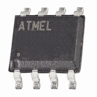
AT24C01BN-SH-B Atmel, AT24C01BN-SH-B Datasheet

AT24C01BN-SH-B
Specifications of AT24C01BN-SH-B
Related parts for AT24C01BN-SH-B
AT24C01BN-SH-B Summary of contents
Page 1
... Description The AT24C01B provides 1024 bits of serial electrically erasable and programmable read-only memory (EEPROM) organized as 128 words of 8 bits each. The device is optimized for use in many industrial and commercial applications where low-power and low-voltage operation are essential. The AT24C01B is available in space-saving ...
Page 2
Absolute Maximum Ratings Operating Temperature..................................–55°C to +125°C Storage Temperature .....................................–65°C to +150°C Voltage on Any Pin with Respect to Ground .................................... –1.0V to +7.0V Maximum Operating Voltage .......................................... 6.25V DC Output Current........................................................ 5.0 mA Figure 1. Block Diagram AT24C01B 2 ...
Page 3
... Pin Description Memory Organization 5156C–SEEPR–4/07 SERIAL CLOCK (SCL): The SCL input is used to positive edge clock data into each EEPROM device and negative edge clock data out of each device. SERIAL DATA (SDA): The SDA pin is bidirectional for serial data transfer. This pin is open-drain driven and may be wire-ORed with any number of other open-drain or open- collector devices ...
Page 4
Table 3. Pin Capacitance Applicable over recommended operating range from T Symbol Test Condition C Input/Output Capacitance (SDA) I/O C Input Capacitance ( Note: 1. This parameter is characterized and is not 100% tested. Table ...
Page 5
Table 5. AC Characteristics Applicable over recommended operating range from T 100 pF (unless otherwise noted) Symbol Parameter f Clock Frequency, SCL SCL t Clock Pulse Width Low LOW t Clock Pulse Width High HIGH t Noise Suppression Time I ...
Page 6
Device Operation AT24C01B 6 CLOCK and DATA TRANSITIONS: The SDA pin is normally pulled high with an exter- nal device. Data on the SDA pin may change only during SCL low time periods (see Figure 4 on page 7). Data ...
Page 7
Bus Timing Figure 2. SCL: Serial Clock, SDA: Serial Data I/O Write Cycle Timing Figure 3. SCL: Serial Clock, SDA: Serial Data I/O SCL SDA 8th BIT WORDn Note: 1. The write cycle time t is the time from a ...
Page 8
Figure 5. Start and Stop Definition Figure 6. Output Acknowledge AT24C01B 8 5156C–SEEPR–4/07 ...
Page 9
... CURRENT ADDRESS READ: The internal data word address counter maintains the last address accessed during the last read or write operation, incremented by one. This address stays valid between operations as long as the chip power is maintained. The address “roll over” during read is from the last byte of the last memory page to the first , to the WR ...
Page 10
... After the microcontroller receives a data word, it responds with an acknowledge. As long as the EEPROM receives an acknowledge, it will continue to increment the data word address and serially clock out sequential data words. When the memory address limit is reached, the data word address will “roll over” and the sequential read will con- tinue ...
Page 11
Figure 7. Device Address Figure 8. Byte Write Figure 9. Page Write * = ( Don’t Care Bit) Figure 10. Current Address Read 5156C–SEEPR–4/ ...
Page 12
Figure 11. Random Read (* = Don’t Care Bit) Figure 12. Sequential Read AT24C01B 12 * 5156C–SEEPR–4/07 ...
Page 13
... AT24C01B Ordering Information Ordering Code AT24C01B-PU (Bulk form only) (1) AT24C01BN-SH-B (NiPdAu Lead Finish) (2) AT24C01BN-SH-T (NiPdAu Lead Finish) (1) AT24C01B-TH-B (NiPdAu Lead Finish) (2) AT24C01B-TH-T (NiPdAu Lead Finish) (2) AT24C01BY6-YH-T (NiPdAu Lead Finish) (2) AT24C01B-TSU-T (2) AT24C01BU3-UU-T (3) AT24C01B-W-11 Notes: 1. “-B” denotes bulk. 2. “-T” denotes tape and reel. SOIC = 4K per reel. TSSOP, Ultra Thin Mini MAP, SOT 23 and dBGA2 = 5K per reel. ...
Page 14
Packaging Information 8P3 – PDIP Top View PLCS Side View Notes: 1. This drawing is for general information only; refer to JEDEC Drawing MS-001, Variation BA, for additional information. 2. Dimensions A and L are measured ...
Page 15
JEDEC SOIC e Side View Note: These drawings are for general information only. Refer to JEDEC Drawing MS-012, Variation AA for proper dimensions, tolerances, datums, etc. 1150 E. Cheyenne Mtn. Blvd. Colorado Springs, CO 80906 R 5156C–SEEPR–4/07 1 ...
Page 16
TSSOP Pin 1 indicator this corner N Top View Side View Notes: 1. This drawing is for general information only. Refer to JEDEC Drawing MO-153, Variation AA, for proper dimensions, tolerances, datums, ...
Page 17
Mini Map D Notes: 1. This drawing is for general information only. Refer to JEDEC Drawing MO-229, for proper dimensions, tolerances, datums, etc. 2. Dimension b applies to metallized terminal and is measured between 0.15 mm and 0.30 ...
Page 18
SOT23 E1 1 Seating Plane NOTES: 1. This drawing is for general information only. Refer to JEDEC Drawing MO-193, Variation AB, for additional information. 2. Dimension D does not include mold flash, protrusions, or gate burrs. Mold flash, ...
Page 19
PIN 1 BALL PAD CORNER Top View PIN 1 BALL PAD CORNER 1 2 (d1 (e1) Bottom View 8 SOLDER BALLS 1. Dimension “b” is measured at the maximum solder ball diameter. This ...
Page 20
Revision History Doc. Rev. 5156C 5156B 5156A AT24C01B 20 Date Comments 4/2007 Removed NC and GND from Pin Configuration; Removed Preliminary from page 1 and all headers/footers; Added 2-wire Software Reset; Removed LSB and MSB from figures; Removed waffle pack ...
Page 21
... Disclaimer: The information in this document is provided in connection with Atmel products. No license, express or implied, by estoppel or otherwise, to any intellectual property right is granted by this document or in connection with the sale of Atmel products. EXCEPT AS SET FORTH IN ATMEL’S TERMS AND CONDI- TIONS OF SALE LOCATED ON ATMEL’S WEB SITE, ATMEL ASSUMES NO LIABILITY WHATSOEVER AND DISCLAIMS ANY EXPRESS, IMPLIED OR STATUTORY WARRANTY RELATING TO ITS PRODUCTS INCLUDING, BUT NOT LIMITED TO, THE IMPLIED WARRANTY OF MERCHANTABILITY, FITNESS FOR A PARTICULAR PURPOSE, OR NON-INFRINGEMENT ...


