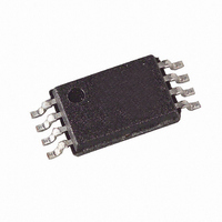
AT24C1024B-TH25-B Atmel, AT24C1024B-TH25-B Datasheet - Page 3

AT24C1024B-TH25-B
Manufacturer Part Number
AT24C1024B-TH25-B
Description
IC EEPROM 1MBIT 1MHZ 8TSSOP
Manufacturer
Atmel
Datasheet
1.AT24C1024BN-SH25-B.pdf
(25 pages)
Specifications of AT24C1024B-TH25-B
Format - Memory
EEPROMs - Serial
Memory Type
EEPROM
Memory Size
1M (128K x 8)
Speed
1MHz
Interface
I²C, 2-Wire Serial
Voltage - Supply
2.5 V ~ 5.5 V
Operating Temperature
-40°C ~ 85°C
Package / Case
8-TSSOP
Organization
128 K x 8
Interface Type
2-Wire
Maximum Clock Frequency
1 MHz
Access Time
550 ns
Supply Voltage (max)
5.5 V
Supply Voltage (min)
2.5 V
Maximum Operating Current
3 mA
Maximum Operating Temperature
+ 85 C
Mounting Style
SMD/SMT
Minimum Operating Temperature
- 40 C
Operating Supply Voltage
3.3 V, 5 V
Lead Free Status / RoHS Status
Lead free / RoHS Compliant
Figure 1-1.
2. Pin Description
5194F–SEEPR–1/08
Block Diagram
GND
VCC
SDA
SCL
WP
A
A
A
2
1
0
SERIAL CLOCK (SCL): The SCL input is used to positive edge clock data into each EEPROM
device and negative edge clock data out of each device.
SERIAL DATA (SDA): The SDA pin is bi-directional for serial data transfer. This pin is open-
drain driven and may be wire-ORed with any number of other open-drain or open-collector
devices.
DEVICE/ADDRESSES (A1/A2): The A1, A2 pin is a device address input that can be hardwired
or left not connected for hardware compatibility with other AT24Cxx devices. When the A1, A2
pins are hardwired, as many as four 1024K devices may be addressed on a single bus system
(device addressing is discussed in detail under the Device Addressing section). If the A1/A2 pins
are left floating, the A1/A2 pin will be internally pulled down to GND if the capacitive coupling to
the circuit board V
A1/A2 pin to GND.
WRITE PROTECT (WP): The write protect input, when connected to GND, allows normal write
operations. When WP is connected high to V
If the pin is left floating, the WP pin will be internally pulled down to GND if the capacitive cou-
pling to the circuit board V
the pin to GND. Switching WP to V
function.
D
IN
COMPARATOR
START
LOGIC
ADDRESS
STOP
DEVICE
CC
LOAD
D
plane is <3 pF. If coupling is >3 pF, Atmel recommends connecting the
OUT
R/W
CC
plane is <3 pF. If coupling is >3 pF, Atmel recommends connecting
ADDR/COUNTER
DATA WORD
COMP
CC
LOAD
Y DEC
prior to a write operation creates a software write-protect
CONTROL
SERIAL
LOGIC
INC
CC
, all write operations to the memory are inhibited.
EN
H.V. PUMP/TIMING
DATA RECOVERY
SERIAL MUX
EEPROM
D
LOGIC
OUT
/ACK
3


