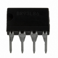
BR93L86-W Rohm Semiconductor, BR93L86-W Datasheet - Page 29

BR93L86-W
Manufacturer Part Number
BR93L86-W
Description
IC EEPROM 16KBIT 2MHZ 8DIP
Manufacturer
Rohm Semiconductor
Datasheet
1.BR93L56RFVM-WTR.pdf
(41 pages)
Specifications of BR93L86-W
Format - Memory
EEPROMs - Serial
Memory Type
EEPROM
Memory Size
16K (1K x 16)
Speed
2MHz
Interface
Microwire, 3-Wire Serial
Voltage - Supply
1.8 V ~ 5.5 V
Operating Temperature
-40°C ~ 85°C
Package / Case
8-DIP (0.300", 7.62mm)
Lead Free Status / RoHS Status
Lead free / RoHS Compliant
Available stocks
Company
Part Number
Manufacturer
Quantity
Price
Company:
Part Number:
BR93L86-W
Manufacturer:
ROHM
Quantity:
2 025
●Timing chart
© 2011 ROHM Co., Ltd. All rights reserved.
BR93L□□-W Series, 93A□□-WM Series, BR93H□□-WC Series
www.rohm.com
*1 Start bit
○When the read command is recognized, input address data (16bit) is output to serial. And at that moment, at taking A0, in
2) Write cycle (WRITE)
○In this command, input 16bit data (D15~D0) are written to designated addresses (Am~A0). The actual write starts by the fall
3) Write all cycyle (WRAL)
○In this command, input 16bit data is written simultaneously to designated block for 128 words. Data is writen in bulk at a
1) Read cycle (READ)
When data “1” is input for the first time after the rise of CS, this is recognized as a start bit. And when “1” is input after plural “0” are input, it is recognized as a
start bit, and the following operation is started. This is common to all the commands to described hereafter
of CS of D0 taken SK clock(n-th clock from the start bit input), to the rise of the (n+1)-th clock.
When STATUS is not detected, (CS="L" fixed) Max. 10ms in conformity with tE/W, and when STATUS is detected (CS="H"),
all commands are not accepted for areas where "L" (BUSY) is output from D0, therefore, do not input any command.
Write is not made even if CS is started after input of clock after (n+1)-th clocks.
Note) Take tSKH or more from the rise of the n-th clock to the fall of CS.
write time of only Max. 10ms in conformity with tE/W. When writing data to all addresses, designate each block by B2, B1,
and B0, and execute write. Write time is Max.10ms. The actual write starts by the fall of CS from the rise of D0 taken at SK
clock (n-th clock from the start bit input), to the rise of the (n+1)-th clock. When CS is ended after clock input after the rise of
the (n+1)-th clock, command is cancelled, and write is not completed.
Note)Take tSKH or more from the rise of the n-th clock to the fall of CS.
CS
SK
DI
DO
sync with the rise of SK, “0” (dummy bit) is output. And, the following data is output in sync with the rise of SK.
This IC has address auto increment function valid only at read command. This is the function where after the above read
execution, by continuously inputting SK clock, the above address data is read sequentially. And, during the auto increment,
keep CS at “H”.
High-Z
DO
CS
SK
DI
DO
CS
SK
DI
High-Z
High-Z
1
*1
1
1
1
1
1
1
2
0
0
2
2
0
1
0
Am
4
Am
0
4
Fig. 31 Write cycle
1
Fig. 30 Read cycle
Fig. 32 Write all cycle
5
~ ~
~ ~
~ ~
~ ~
~ ~
~ ~
~ ~
~ ~
~ ~
A1
A1
B2
m
A0
A0
B1
0
D15
D15 D14
B0
D14
D15
~ ~
~ ~
~ ~
~ ~
29/40
D1
~ ~
~ ~
~ ~
~ ~
D1
D1
D0
tCS
n
D0
n
D0
tCS
n
tE/W
n+1
D15 D14
*2
BUSY
tSV
tE/W
~ ~
~ ~
~ ~
~ ~
~ ~
STATUS
tSV
BUSY
READY
STATUS
~ ~
~ ~
READY
~ ~
~ ~
.
*2 The following address data output
( auto increment function )
BR93H56/66-WC : n=27, m=7
BR93H76/86-WC : n=29, m=9
BR93H56/66-WC : n=27, m=7
BR93H76/86-WC : n=29, m=9
BR93H56/66-WC : n=27, m=9
BR93H76/86-WC : n=29, m=11
Technical Note
2011.02 - Rev.F


