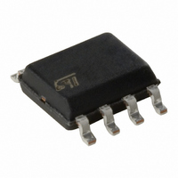
M95512-RMN6TP STMicroelectronics, M95512-RMN6TP Datasheet - Page 27

M95512-RMN6TP
Manufacturer Part Number
M95512-RMN6TP
Description
IC EEPROM 512KBIT 2MHZ 8SOIC
Manufacturer
STMicroelectronics
Specifications of M95512-RMN6TP
Format - Memory
EEPROMs - Serial
Memory Type
EEPROM
Memory Size
512K (64K x 8)
Speed
2MHz
Interface
SPI, 3-Wire Serial
Voltage - Supply
1.8 V ~ 5.5 V
Operating Temperature
-40°C ~ 85°C
Package / Case
8-SOIC (3.9mm Width)
Density
512Kb
Interface Type
Serial (SPI)
Organization
64Kx8
Access Time (max)
150ns
Frequency (max)
2MHz
Write Protection
Yes
Data Retention
40Year
Operating Supply Voltage (typ)
2.5/3.3/5V
Operating Temp Range
-40C to 85C
Supply Current
3mA
Operating Supply Voltage (min)
1.8V
Operating Supply Voltage (max)
5.5V
Operating Temperature Classification
Industrial
Mounting
Surface Mount
Pin Count
8
Lead Free Status / RoHS Status
Lead free / RoHS Compliant
Other names
497-6356-2
Available stocks
Company
Part Number
Manufacturer
Quantity
Price
Company:
Part Number:
M95512-RMN6TP
Manufacturer:
TDK
Quantity:
324
M95512-DR, M95512-W, M95512-R
6.8
Write Identification Page (available only in M95512-DR
devices)
The Identification Page (128 bytes) is an additional page which can be written and (later)
permanently locked in Read-only mode. Writing this page is achieved with the Write
Identification Page instruction (see
bits of the instruction byte, address byte, and at least one data byte are then shifted in on
Serial Data input (D). Address bit A10 must be 0, address bits [A15:A11] and [A9:A7] are
Don't Care, the [A6:A0] address bits define the byte address inside the identification page.
The instruction is terminated by driving Chip Select (S) high at a byte boundary of the input
data. The self-timed write cycle triggered by the rising edge of Chip Select (S) continues for
a period t
(WIP) bit is reset to 0.
In the case of
has been latched in, indicating that the instruction is being used to write a single byte.
However, if Chip Select (S) continues to be driven low, as shown in
of input data is shifted in, so that more than a single byte, starting from the given address
towards the end of the same page, can be written in a single internal write cycle. Each time
a new data byte is shifted in, the least significant bits of the internal address counter are
incremented. If the number of data bytes sent to the device exceeds the page boundary, the
internal address counter rolls over to the beginning of the page, and the previous data there
are overwritten with the incoming data. (The page size of these devices is 128 bytes).
The instruction is not accepted, and is not executed, under the following conditions:
●
●
●
●
●
Figure 16. Write Identification Page sequence
if the Write Enable Latch (WEL) bit has not been set to 1 (by previously executing a
Write Enable instruction)
if Status register bits (BP1, BP0) = (1, 1)
if a write cycle is already in progress
if the device has not been deselected, by Chip Select (S) being driven high, at a byte
boundary (after the eighth bit, b0, of the last data byte that was latched in)
if the Identification page is locked by the Lock Status bit
W
(as specified in
Figure
16, Chip Select (S) is driven high after the eighth bit of the data byte
Table 18
Doc ID 11124 Rev 14
Table
and
Table
4), the Chip Select signal (S) is first driven low. The
19), at the end of which the Write in Progress
Figure
16, the next byte
Instructions
27/48


