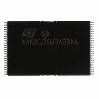
NAND128W3A2BN6E NUMONYX, NAND128W3A2BN6E Datasheet - Page 53

NAND128W3A2BN6E
Manufacturer Part Number
NAND128W3A2BN6E
Description
IC FLASH 128MBIT 48TSOP
Manufacturer
NUMONYX
Specifications of NAND128W3A2BN6E
Format - Memory
FLASH
Memory Type
FLASH - Nand
Memory Size
128M (16M x 8)
Interface
Parallel
Voltage - Supply
2.7 V ~ 3.6 V
Operating Temperature
-40°C ~ 85°C
Package / Case
48-TSOP
Access Time
12µs
Supply Voltage Range
2.7V To 3.6V
Memory Case Style
TSOP
No. Of Pins
48
Operating Temperature Range
-40°C To +85°C
Voltage, Vcc
3.3V
Rohs Compliant
Yes
Lead Free Status / RoHS Status
Lead free / RoHS Compliant
Speed
-
Lead Free Status / RoHS Status
Lead free / RoHS Compliant, Lead free / RoHS Compliant
Other names
497-5037
497-5037
497-5037
Available stocks
Company
Part Number
Manufacturer
Quantity
Price
Company:
Part Number:
NAND128W3A2BN6E
Manufacturer:
MICRON
Quantity:
3 000
Part Number:
NAND128W3A2BN6E
Manufacturer:
ST
Quantity:
20 000
APPENDIX A. HARDWARE INTERFACE EXAMPLES
Nand Flash devices can be connected to a micro-
controller system bus for code and data storage.
For microcontrollers that have an embedded
NAND controller the NAND Flash can be connect-
ed without the addition of glue logic (see
Figure
required for general purpose microcontrollers that
do not have an embedded NAND controller. The
glue logic usually consists of a flip-flop to hold the
Chip Enable, Address Latch Enable and Com-
mand Latch Enable signals stable during com-
mand and address latch operations, and some
logic gates to simplify the firmware or make the de-
sign more robust.
Figure 46.
NAND Flash to a general purpose microcontroller.
The additional OR gates allow the microcontrol-
ler’s Output Enable and Write Enable signals to be
used for other peripherals. The OR gate between
Figure 45. Connection to Microcontroller, Without Glue Logic
45.). However a minimum of glue logic is
gives an example of how to connect a
Microcontroller
AD(24:16)
PWAITEN
CSn
DQ
G
W
V DD or V SS
or General Purpose I/O
NAND128-A, NAND256-A, NAND512-A, NAND01G-A
A3 and CSn maps the flip-flop and NAND I/O in
different address spaces inside the same chip se-
lect unit, which improves the setup and hold times
and simplifies the firmware. The structure uses the
microcontroller DMA (Direct Memory Access) en-
gines to optimize the transfer between the NAND
Flash and the system RAM.
For any interface with glue logic, the extra delay
caused by the gates and flip-flop must be taken
into account. This delay must be added to the mi-
crocontroller’s AC characteristics and register set-
tings to get the NAND Flash setup and hold times.
For mass storage applications (hard disk emula-
tions or systems where a huge amount of storage
is required) NAND Flash memories can be con-
nected together to build storage modules (see
ure
AD17
AD16
47.).
V DD
AL
CL
R
W
E
I/O
RB
WP
NAND
Flash
AI08045b
53/56
Fig-


