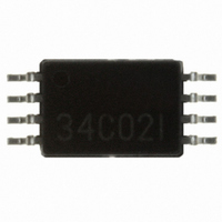
CAT34C02YI-G ON Semiconductor, CAT34C02YI-G Datasheet - Page 5

CAT34C02YI-G
Manufacturer Part Number
CAT34C02YI-G
Description
IC EEPROM 2KBIT 400KHZ 8TSSOP
Manufacturer
ON Semiconductor
Datasheet
1.CAT34C02VP2I-GT4.pdf
(14 pages)
Specifications of CAT34C02YI-G
Format - Memory
EEPROMs - Serial
Memory Type
EEPROM
Memory Size
2K (256 x 8)
Speed
400kHz
Interface
I²C, 2-Wire Serial
Voltage - Supply
1.7 V ~ 5.5 V
Operating Temperature
-40°C ~ 85°C
Package / Case
8-TSSOP
Organization
256 K x 8
Interface Type
I2C
Maximum Clock Frequency
0.4 MHz
Access Time
900 ns
Supply Voltage (max)
5.5 V
Supply Voltage (min)
1.7 V
Maximum Operating Current
1 mA
Maximum Operating Temperature
+ 85 C
Mounting Style
SMD/SMT
Minimum Operating Temperature
- 40 C
Operating Supply Voltage
1.8 V , 2.5 V , 3.3 V , 5 V
Lead Free Status / RoHS Status
Lead free / RoHS Compliant
Other names
34C02YI-G
Available stocks
Company
Part Number
Manufacturer
Quantity
Price
Company:
Part Number:
CAT34C02YI-GT3
Manufacturer:
CATALYST
Quantity:
5 388
Part Number:
CAT34C02YI-GT3
Manufacturer:
CATALYST
Quantity:
20 000
Company:
Part Number:
CAT34C02YI-GT5
Manufacturer:
ON Semiconductor
Quantity:
3 950
Write Operations
Byte Write
by Slave address, byte address and data to be written
(Figure 6). The Slave acknowledges all 3 bytes, and the
Master then follows up with a STOP, which in turn starts the
internal Write operation (Figure 7). During internal Write,
the Slave will not acknowledge any Read or Write request
from the Master.
Page Write
pages of 16 bytes each. A page is selected by the 4 most
significant bits of the address byte following the Slave
address, while the 4 least significant bits point to the byte
within the page. Up to 16 bytes can be written in one Write
cycle (Figure 8).
SDA OUT
In Byte Write mode the Master sends a START, followed
The CAT34C02 contains 256 bytes of data, arranged in 16
FROM TRANSMITTER
SDA IN
SCL
FROM RECEIVER
DATA OUTPUT
DATA OUTPUT
SCL FROM
MASTER
t
SU:STA
START
t
F
BUS RELEASE DELAY (TRANSMITTER)
t
HD:STA
t
LOW
1
1
t
Figure 4. Acknowledge Timing
AA
0
Figure 3. Slave Address Bits
t
HD:DAT
t
HIGH
Figure 5. Bus Timing
1
http://onsemi.com
ACK DELAY (≤ t
0
5
t
LOW
DEVICE ADDRESS
A
incremented after each data byte is loaded. If the Master
transmits more than 16 data bytes, then earlier bytes will be
overwritten by later bytes in a ‘wrap−around’ fashion
(within the selected page). The internal Write cycle starts
immediately following the STOP.
Acknowledge Polling
CAT34C02 is busy writing or is ready to accept commands.
Polling is implemented by interrogating the device with a
‘Selective Read’ command (see READ OPERATIONS).
as long as internal Write is in progress.
Delivery State
flag is set. The entire 2 kb memory is erased, i.e. all bytes are
FFh.
2
AA
The internal byte address counter is automatically
Acknowledge polling can be used to determine if the
The CAT34C02 will not acknowledge the Slave address,
The CAT34C02 is shipped ‘unprotected’, i.e. neither SWP
t
DH
)
A
8
1
t
SU:DAT
t
R
A
0
R/W
9
ACK SETUP (≥ t
BUS RELEASE DELAY
(RECEIVER)
t
SU:DAT
t
BUF
SU:STO
)


