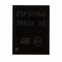
M25P32-VME6TG NUMONYX, M25P32-VME6TG Datasheet - Page 25

M25P32-VME6TG
Manufacturer Part Number
M25P32-VME6TG
Description
IC FLASH 32MBIT 75MHZ 8VDFPN
Manufacturer
NUMONYX
Series
Forté™r
Datasheet
1.M25P32-VME6G.pdf
(54 pages)
Specifications of M25P32-VME6TG
Format - Memory
FLASH
Memory Type
FLASH
Memory Size
32M (4M x 8)
Speed
75MHz
Interface
SPI, 3-Wire Serial
Voltage - Supply
2.7 V ~ 3.6 V
Operating Temperature
-40°C ~ 85°C
Package / Case
8-VDFPN
Lead Free Status / RoHS Status
Lead free / RoHS Compliant
Other names
M25P32-VME6TG
M25P32-VME6TGTR
M25P32-VME6TGTR
Available stocks
Company
Part Number
Manufacturer
Quantity
Price
Company:
Part Number:
M25P32-VME6TG
Manufacturer:
MICRON
Quantity:
1 000
Company:
Part Number:
M25P32-VME6TG
Manufacturer:
NUMONYX
Quantity:
12 550
Part Number:
M25P32-VME6TG
Manufacturer:
MICRON
Quantity:
20 000
6.4.4
6.5
BP1, BP0) bits is set to 1, the relevant memory area (as defined in
protected against Page Program (PP) and Sector Erase (SE) instructions. The Block Protect
(BP2, BP1, BP0) bits can be written provided that the Hardware Protected mode has not
been set. The Bulk Erase (BE) instruction is executed if, and only if, all Block Protect (BP2,
BP1, BP0) bits are 0.
SRWD bit
The Status Register Write Disable (SRWD) bit is operated in conjunction with the Write
Protect (W/V
(W/V
Register Write Disable (SRWD) bit is set to 1, and Write Protect (W/V
this mode, the non-volatile bits of the Status Register (SRWD, BP2, BP1, BP0) become
read-only bits and the Write Status Register (WRSR) instruction is no longer accepted for
execution.
Figure 11. Read Status Register (RDSR) instruction sequence and data-out
Write Status Register (WRSR)
The Write Status Register (WRSR) instruction allows new values to be written to the Status
Register. Before it can be accepted, a Write Enable (WREN) instruction must previously
have been executed. After the Write Enable (WREN) instruction has been decoded and
executed, the device sets the Write Enable Latch (WEL).
The Write Status Register (WRSR) instruction is entered by driving Chip Select (S) Low,
followed by the instruction code and the data byte on Serial Data Input (D).
The instruction sequence is shown in
The Write Status Register (WRSR) instruction has no effect on b6, b5, b1 and b0 of the
Status Register. b6 and b5 are always read as 0.
Chip Select (S) must be driven High after the eighth bit of the data byte has been latched in.
If not, the Write Status Register (WRSR) instruction is not executed. As soon as Chip Select
(S) is driven High, the self-timed Write Status Register cycle (whose duration is t
initiated. While the Write Status Register cycle is in progress, the Status Register may still
be read to check the value of the Write In Progress (WIP) bit. The Write In Progress (WIP)
S
C
D
Q
PP
) signal allow the device to be put in the Hardware Protected mode (when the Status
PP
sequence
0
High Impedance
) signal. The Status Register Write Disable (SRWD) bit and Write Protect
1
2
Instruction
3
4
5
6
7
MSB
7
8
Figure
6
Status Register Out
9 10 11 12 13 14 15
5
4
12.
3
2
1
0
MSB
7
6
Status Register Out
5
Table
4
PP
3
) is driven Low). In
2) becomes
2
1
0
W
) is
7
AI02031E
25/54


