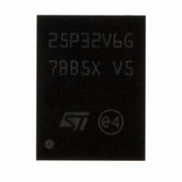
M25P32-VME6TG NUMONYX, M25P32-VME6TG Datasheet - Page 26

M25P32-VME6TG
Manufacturer Part Number
M25P32-VME6TG
Description
IC FLASH 32MBIT 75MHZ 8VDFPN
Manufacturer
NUMONYX
Series
Forté™r
Datasheet
1.M25P32-VME6G.pdf
(54 pages)
Specifications of M25P32-VME6TG
Format - Memory
FLASH
Memory Type
FLASH
Memory Size
32M (4M x 8)
Speed
75MHz
Interface
SPI, 3-Wire Serial
Voltage - Supply
2.7 V ~ 3.6 V
Operating Temperature
-40°C ~ 85°C
Package / Case
8-VDFPN
Lead Free Status / RoHS Status
Lead free / RoHS Compliant
Other names
M25P32-VME6TG
M25P32-VME6TGTR
M25P32-VME6TGTR
Available stocks
Company
Part Number
Manufacturer
Quantity
Price
Company:
Part Number:
M25P32-VME6TG
Manufacturer:
MICRON
Quantity:
1 000
Company:
Part Number:
M25P32-VME6TG
Manufacturer:
NUMONYX
Quantity:
12 550
Part Number:
M25P32-VME6TG
Manufacturer:
MICRON
Quantity:
20 000
26/54
bit is 1 during the self-timed Write Status Register cycle, and is 0 when it is completed.
When the cycle is completed, the Write Enable Latch (WEL) is reset.
The Write Status Register (WRSR) instruction allows the user to change the values of the
Block Protect (BP2, BP1, BP0) bits, to define the size of the area that is to be treated as
read-only, as defined in
the user to set or reset the Status Register Write Disable (SRWD) bit in accordance with the
Write Protect (W/V
Protect (W/V
The Write Status Register (WRSR) instruction is not executed once the Hardware Protected
Mode (HPM) is entered.
Figure 12. Write Status Register (WRSR) instruction sequence
Table 7.
1. As defined by the values in the Block Protect (BP2, BP1, BP0) bits of the Status Register, as shown in
The protection features of the device are summarized in
When the Status Register Write Disable (SRWD) bit of the Status Register is 0 (its initial
delivery state), it is possible to write to the Status Register provided that the Write Enable
W/V
signal
Table
1
0
1
0
PP
2.
SRWD
bit
0
0
1
1
S
C
D
Q
PP
Protection modes
) signal allow the device to be put in the Hardware Protected Mode (HPM).
Protected
Hardware
Protected
Software
(SPM)
(HPM)
Mode
PP
) signal. The Status Register Write Disable (SRWD) bit and Write
Table
0
Status Register is
Writable (if the WREN
instruction has set the
WEL bit)
The values in the SRWD,
BP2, BP1 and BP0 bits
can be changed
Status Register is
Hardware write protected
The values in the SRWD,
BP2, BP1 and BP0 bits
cannot be changed
Write Protection of the
1
High Impedance
2. The Write Status Register (WRSR) instruction also allows
Status Register
2
Instruction
3
4
5
6
7
MSB
7
8
6
Protected against
Page Program,
Sector Erase and
Bulk Erase
Protected against
Page Program,
Sector Erase and
Bulk Erase
9 10 11 12 13 14 15
Protected area
5
Register In
Table
4
Status
3
2
7.
Memory content
1
(1)
0
Unprotected area
Ready to accept
Page Program and
Sector Erase
instructions
Ready to accept
Page Program and
Sector Erase
instructions
AI02282D
(1)


