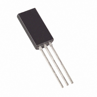
DS2433+ Maxim Integrated Products, DS2433+ Datasheet - Page 4

DS2433+
Manufacturer Part Number
DS2433+
Description
IC EEPROM 4KBIT TO92-3
Manufacturer
Maxim Integrated Products
Datasheet
1.DS2433.pdf
(23 pages)
Specifications of DS2433+
Format - Memory
EEPROMs - Serial
Memory Type
EEPROM
Memory Size
4K (256 x 16)
Interface
1-Wire Serial
Operating Temperature
-40°C ~ 85°C
Package / Case
TO-92-3 (Long Body), TO-226
Organization
4 K x 1
Interface Type
1-Wire
Supply Voltage (max)
6 V
Supply Voltage (min)
2.8 V
Maximum Operating Current
500 uA
Maximum Operating Temperature
+ 85 C
Mounting Style
Through Hole
Minimum Operating Temperature
- 40 C
Lead Free Status / RoHS Status
Lead free / RoHS Compliant
Voltage - Supply
-
Speed
-
Lead Free Status / Rohs Status
Lead free / RoHS Compliant
DS2433
the PF bit. Bit 6 has no function; it always reads 0. Note that the lowest five bits of the target address also
determine the address within the scratchpad, where intermediate storage of data will begin. This address
is called byte offset. If the target address (TA1) for a Write command is 03Ch for example, then the
scratchpad will store incoming data beginning at the byte offset 1Ch and will be full after only four bytes.
The corresponding ending offset in this example is 1Fh. For best economy of speed and efficiency, the
target address for writing should point to the beginning of a new page, i.e., the byte offset will be 0. Thus
the full 32-byte capacity of the scratchpad is available, resulting also in the ending offset of 1Fh.
However, it is possible to write one or several contiguous bytes somewhere within a page. The ending
offset together with the Partial Flag support the master checking the data integrity after a Write command.
The highest valued bit of the E/S register, called AA is valid only if the PF flag reads 0. If PF is 0 and AA
is 1, a copy has taken place. The AA bit is cleared when the device receives a write scratchpad command.
WRITING WITH VERIFICATION
To write data to the DS2433, the scratchpad has to be used as intermediate storage. First the master issues
the Write Scratchpad command to specify the desired target address, followed by the data to be written to
the scratchpad. Under certain conditions (see Write Scratchpad command) the master will receive an
inverted CRC16 of the command, address and data at the end of the write scratchpad command sequence.
Knowing this CRC value, the master can compare it to the value it has calculated itself to decide if the
communication was successful and proceed to the Copy Scratchpad command. If the master could not
receive the CRC16, it has to send the Read Scratchpad command to read back the scratchpad to verify
data integrity. As preamble to the scratchpad data, the DS2433 repeats the target address TA1 and TA2
and sends the contents of the E/S register. If the PF flag is set, data did not arrive correctly in the
scratchpad or there was a loss of power since data was last written to the scratchpad. The master does not
need to continue reading; it can start a new trial to write data to the scratchpad. Similarly, a set AA flag
together with a cleared PF flag indicates that the Write command was not recognized by the device. If
everything went correctly, both flags are cleared and the ending offset indicates the address of the last
byte written to the scratchpad. Now the master can continue reading and verifying every data byte. After
the master has verified the data, it has to send the Copy Scratchpad command. This command must be
followed exactly by the data of the three address registers TA1, TA2 and E/S. The master may obtain the
contents of these registers by reading the scratchpad or derive it from the target address and the amount of
data to be written. As soon as the DS2433 has received these bytes correctly, it will copy the data to the
requested location beginning at the target address.
4 of 23


