M25PE80-VMN6TP NUMONYX, M25PE80-VMN6TP Datasheet - Page 12
M25PE80-VMN6TP
Manufacturer Part Number
M25PE80-VMN6TP
Description
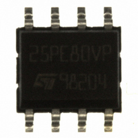
IC FLASH 8MBIT 75MHZ 8SOIC
Manufacturer
NUMONYX
Series
Forté™r
Datasheet
1.M25PE80-VMN6TP.pdf
(66 pages)
Specifications of M25PE80-VMN6TP
Format - Memory
FLASH
Memory Type
FLASH
Memory Size
8M (1M x 8)
Speed
75MHz
Interface
SPI, 3-Wire Serial
Voltage - Supply
2.7 V ~ 3.6 V
Operating Temperature
-40°C ~ 85°C
Package / Case
8-SOIC (3.9mm Width)
Package
8SOIC N
Cell Type
NOR
Density
8 Mb
Architecture
Sectored
Block Organization
Symmetrical
Typical Operating Supply Voltage
3.3 V
Sector Size
256Byte x 4096
Timing Type
Synchronous
Interface Type
Serial-SPI
Lead Free Status / RoHS Status
Lead free / RoHS Compliant
Other names
M25PE80-VMN6TPTR
Available stocks
Company
Part Number
Manufacturer
Quantity
Price
Company:

Part Number:
M25PE80-VMN6TP
Manufacturer:
ST
Quantity:
6 000
Part Number:
M25PE80-VMN6TP
Manufacturer:
ST
Quantity:
20 000


Operating features
4
4.1
4.2
12/66
Operating features
Sharing the overhead of modifying data
To write or program one (or more) data bytes, two instructions are required: write enable
(WREN), which is one byte, and a page write (PW) or page program (PP) sequence, which
consists of four bytes plus data. This is followed by the internal cycle (of duration t
To share this overhead, the page write (PW) or page program (PP) instruction allows up to
256 bytes to be programmed (changing bits from 1 to 0) or written (changing bits to 0 or 1) at
a time, provided that they lie in consecutive addresses on the same page of memory.
An easy way to modify data
The page write (PW) instruction provides a convenient way of modifying data (up to 256
contiguous bytes at a time), and simply requires the start address, and the new data in the
instruction sequence.
The page write (PW) instruction is entered by driving Chip Select (S) Low, and then
transmitting the instruction byte, three address bytes (A23-A0) and at least one data byte,
and then driving Chip Select (S) High. While Chip Select (S) is being held Low, the data
bytes are written to the data buffer, starting at the address given in the third address byte
(A7-A0). When Chip Select (S) is driven High, the write cycle starts. The remaining,
unchanged, bytes of the data buffer are automatically loaded with the values of the
corresponding bytes of the addressed memory page. The addressed memory page then
automatically put into an erase cycle. Finally, the addressed memory page is programmed
with the contents of the data buffer.
All of this buffer management is handled internally, and is transparent to the user. The user
is given the facility of being able to alter the contents of the memory on a byte-by-byte basis.
For optimized timings, it is recommended to use the page write (PW) instruction to write all
consecutive targeted bytes in a single sequence versus using several page write (PW)
sequences with each containing only a few bytes (see
Table 22: AC
(0.11 µm)
process)).
characteristics, and
Table 24: AC characteristics (75 MHz operation, T9HX
Section 6.9: Page write
(PW),
PW
M25PE80
or t
PP
).
Related parts for M25PE80-VMN6TP
Image
Part Number
Description
Manufacturer
Datasheet
Request
R

Part Number:
Description:
IC FLASH 8MBIT 75MHZ 8VFQFPN
Manufacturer:
NUMONYX
Datasheet:

Part Number:
Description:
IC FLASH 8MBIT 75MHZ 8SOIC
Manufacturer:
NUMONYX
Datasheet:
Part Number:
Description:
Flash Mem Serial-SPI 3.3V 8M-Bit 1M x 8 8ns 8-Pin SOIC N Tray
Manufacturer:
NUMONYX
Datasheet:
Part Number:
Description:
IC SRL FLASH 8MB PG ERS 3V QFN8L
Manufacturer:
NUMONYX
Datasheet:
Part Number:
Description:
Manufacturer:
NUMONYX
Datasheet:

Part Number:
Description:
8-Mbit, page-erasable serial flash memory with byte alterability, 75 MHz SPI bus, standard pinout
Manufacturer:
Numonyx, B.V.
Datasheet:
Part Number:
Description:
8-Mbit, page-erasable serial flash memory with byte alterability, 75 MHz SPI bus, standard pinout
Manufacturer:
Numonyx, B.V.
Datasheet:
Part Number:
Description:
8-Mbit, page-erasable serial flash memory with byte alterability, 75 MHz SPI bus, standard pinout
Manufacturer:
Numonyx, B.V.
Datasheet:
Part Number:
Description:
Numonyx� Embedded Flash Memory J3 V. D
Manufacturer:
Numonyx
Datasheet: