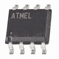
AT26DF081A-SU Atmel, AT26DF081A-SU Datasheet - Page 25

AT26DF081A-SU
Manufacturer Part Number
AT26DF081A-SU
Description
IC FLASH 8MBIT 70MHZ 8SOIC
Manufacturer
Atmel
Datasheet
1.AT26DF081A-SU.pdf
(40 pages)
Specifications of AT26DF081A-SU
Format - Memory
FLASH
Memory Type
DataFLASH
Memory Size
8M (4096 pages x 256 bytes)
Speed
70MHz
Interface
SPI, 3-Wire Serial
Voltage - Supply
2.7 V ~ 3.6 V
Operating Temperature
-40°C ~ 85°C
Package / Case
8-SOIC (5.3mm Width), 8-SOP, 8-SOEIAJ
Lead Free Status / RoHS Status
Lead free / RoHS Compliant
Other names
AT26DF081-SU
AT26DF081-SU
AT26DF081-SU
Available stocks
Company
Part Number
Manufacturer
Quantity
Price
Company:
Part Number:
AT26DF081A-SU
Manufacturer:
ATMEL
Quantity:
12 000
Part Number:
AT26DF081A-SU
Manufacturer:
ATMEL/爱特梅尔
Quantity:
20 000
10.1.6
10.1.7
3600G–DFLASH–06/09
WEL Bit
RDY/BSY Bit
The WEL bit indicates the current status of the internal Write Enable Latch. When the WEL bit is
in the logical “0” state, the device will not accept any program, erase, Protect Sector, Unprotect
Sector, or Write Status Register commands. The WEL bit defaults to the logical “0” state after a
device power-up or reset. In addition, the WEL bit will be reset to the logical “0” state automati-
cally under the following conditions:
If the WEL bit is in the logical “1” state, it will not be reset to a logical “0” if an operation aborts
due to an incomplete or unrecognized opcode being clocked into the device before the CS pin is
deasserted. In order for the WEL bit to be reset when an operation aborts prematurely, the entire
opcode for a program, erase, Protect Sector, Unprotect Sector, or Write Status Register com-
mand must have been clocked into the device.
The RDY/BSY bit is used to determine whether or not an internal operation, such as a program
or erase, is in progress. To poll the RDY/BSY bit to detect the completion of a program or erase
cycle, new Status Register data must be continually clocked out of the device until the state of
the RDY/BSY bit changes from a logical “1” to a logical “0”.
Figure 10-1. Read Status Register
• Write Disable operation completes successfully
• Write Status Register operation completes successfully or aborts
• Protect Sector operation completes successfully or aborts
• Unprotect Sector operation completes successfully or aborts
• Byte/Page Program operation completes successfully or aborts
• Sequential Program Mode reaches highest unprotected memory location
• Sequential Program Mode reaches the end of the memory array
• Sequential Program Mode aborts
• Block Erase operation completes successfully or aborts
• Chip Erase operation completes successfully or aborts
• Hold condition aborts
SCK
SO
CS
SI
HIGH-IMPEDANCE
MSB
0
0
0
1
0
2
OPCODE
0
3
0
4
1
5
0
6
1
7
MSB
D
STATUS REGISTER DATA
8
D
9
D
10 11
D
D
12
D
13 14
D
D
15 16
MSB
D
STATUS REGISTER DATA
D
17
D
18
D
19
D
20
D
21 22
D
D
23 24
MSB
D
D
25


