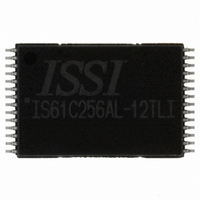
IS61C256AL-12TLI ISSI, Integrated Silicon Solution Inc, IS61C256AL-12TLI Datasheet - Page 6

IS61C256AL-12TLI
Manufacturer Part Number
IS61C256AL-12TLI
Description
IC SRAM 256KBIT 12NS 28TSOP
Manufacturer
ISSI, Integrated Silicon Solution Inc
Type
Asynchronousr
Datasheet
1.IS61C256AL-12JLI.pdf
(12 pages)
Specifications of IS61C256AL-12TLI
Memory Size
256K (32K x 8)
Package / Case
28-TSOP
Interface
Parallel
Format - Memory
RAM
Memory Type
SRAM - Asynchronous
Speed
12ns
Voltage - Supply
4.5 V ~ 5.5 V
Operating Temperature
-40°C ~ 85°C
Access Time
12 ns
Supply Voltage (max)
5.5 V
Supply Voltage (min)
4.5 V
Maximum Operating Current
25 mA
Organization
32 K x 8
Maximum Operating Temperature
+ 85 C
Minimum Operating Temperature
- 40 C
Mounting Style
SMD/SMT
Number Of Ports
1
Operating Supply Voltage
5 V
Density
256Kb
Access Time (max)
12ns
Sync/async
Asynchronous
Architecture
Not Required
Clock Freq (max)
Not RequiredMHz
Operating Supply Voltage (typ)
5V
Address Bus
15b
Package Type
TSOP-I
Operating Temp Range
-40C to 85C
Supply Current
25mA
Operating Supply Voltage (min)
4.5V
Operating Supply Voltage (max)
5.5V
Operating Temperature Classification
Industrial
Mounting
Surface Mount
Pin Count
28
Word Size
8b
Number Of Words
32K
Lead Free Status / RoHS Status
Lead free / RoHS Compliant
Lead Free Status / RoHS Status
Lead free / RoHS Compliant, Lead free / RoHS Compliant
Other names
706-1031
Available stocks
Company
Part Number
Manufacturer
Quantity
Price
Company:
Part Number:
IS61C256AL-12TLI
Manufacturer:
ISSI
Quantity:
6 447
Company:
Part Number:
IS61C256AL-12TLI
Manufacturer:
ISSI
Quantity:
135
Company:
Part Number:
IS61C256AL-12TLI
Manufacturer:
ISSI
Quantity:
1 301
Part Number:
IS61C256AL-12TLI
Manufacturer:
ISSI
Quantity:
20 000
IS61C256AL
WRITE CYCLE SWITCHING CHARACTERISTICS
Notes:
1. Test conditions assume signal transition times of 3 ns or less, timing reference levels of 1.5V, input pulse levels of 0 to 3.0V and
2. Tested with the load in Figure 2. Transition is measured ±500 mV from steady-state voltage. Not 100% tested.
3. The internal write time is defined by the overlap of CE LOW and WE LOW. All signals must be in valid states to initiate a Write,
AC WAVEFORMS
WRITE CYCLE NO. 1 (WE
6
ADDRESS
Symbol
output loading specified in Figure 1.
but any one can go inactive to terminate the Write. The Data Input Setup and Hold timing are referenced to the rising or falling
edge of the signal that terminates the write.
t
t
t
t
t
t
t
t
t
t
t
WC
SCS
AW
HA
SA
PWE
PWE
SD
HD
HZWE
LZWE
D
1
2
OUT
WE
D
(2)
(2)
CE
IN
Parameter
Write Cycle Time
CE to Write End
Address Setup Time
to Write End
Address Hold
from Write End
Address Setup Time
WE Pulse Width (OE LOW)
WE Pulse Width (OE HIGH)
Data Setup to Write End
Data Hold from Write End
WE LOW to High-Z Output
WE HIGH to Low-Z Output
DATA UNDEFINED
t
SA
WE
WE
WE
WE Controlled)
(1,2)
Integrated Silicon Solution, Inc. — www.issi.com —
t
HZWE
t
VALID ADDRESS
AW
t
t
Min.
PWE1
PWE2
10
—
9
9
0
0
9
8
7
0
0
-10 ns
t
t
SCS
WC
(1,3)
Max
HIGH-Z
—
—
—
—
—
—
—
—
—
—
6
(Over Operating Range)
t
SD
DATA
Min. Max.
12
10
10
—
IN
0
0
9
8
7
0
0
-12 ns
VALID
—
—
—
—
—
—
—
—
—
—
6
t
HD
t
LZWE
t
HA
Unit
ns
ns
ns
ns
ns
ns
ns
ns
ns
ns
ns
ISSI
1-800-379-4774
CE_WR1.eps
10/23/06
Rev. B
®


