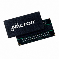
MT47H32M8BP-5E:B TR Micron Technology Inc, MT47H32M8BP-5E:B TR Datasheet - Page 122

MT47H32M8BP-5E:B TR
Manufacturer Part Number
MT47H32M8BP-5E:B TR
Description
IC DDR2 SDRAM 256MBIT 5NS 60FBGA
Manufacturer
Micron Technology Inc
Datasheet
1.MT47H16M16BG-3B_TR.pdf
(128 pages)
Specifications of MT47H32M8BP-5E:B TR
Format - Memory
RAM
Memory Type
DDR2 SDRAM
Memory Size
256M (32M x 8)
Speed
5ns
Interface
Parallel
Voltage - Supply
1.7 V ~ 1.9 V
Operating Temperature
0°C ~ 85°C
Package / Case
60-FBGA
Lead Free Status / RoHS Status
Lead free / RoHS Compliant
ODT Timing
PDF: 09005aef8117c187
256MbDDR2.pdf - Rev. M 7/09 EN
Once a 12ns delay (
bled via the EMR LOAD MODE command, ODT can be accessed under two timing
categories. ODT will operate either in synchronous mode or asynchronous mode, de-
pending on the state of CKE. ODT can switch anytime except during self refresh mode
and a few clocks after being enabled via EMR, as shown in Figure 79 (page 123).
There are two timing categories for ODT—turn-on and turn-off. During active mode
(CKE HIGH) and fast-exit power-down mode (any row of any bank open, CKE LOW,
MR[12 = 0]),
in Figure 81 (page 124).
During slow-exit power-down mode (any row of any bank open, CKE LOW, MR[12] = 1)
and precharge power-down mode (all banks/rows precharged and idle, CKE LOW),
t
ODT turn-off timing, prior to entering any power-down mode, is determined by the pa-
rameter
signal satisfies
(MIN) is satisfied,
shows the example where
occur until state T3. When
ODT turn-on timing prior to entering any power-down mode is determined by the pa-
rameter
satisfies
satisfied,
the example where
until state T3. When
ODT turn-off timing after exiting any power-down mode is determined by the parame-
ter
satisfies
satisfied,
the example where
When
ODT turn-on timing after exiting either slow-exit power-down mode or precharge power-
down mode is determined by the parameter
(page 128). At state Ta1, the ODT HIGH signal satisfies
down mode at state T1. When
parameters apply. Figure 86 (page 128) also shows the example where
not satisfied because ODT HIGH occurs at state Ta0. When
t
AONPD and
AONPD timing parameters apply.
t
AXPD (MIN), as shown in Figure 85 (page 127). At state Ta1, the ODT LOW signal
t
AXPD (MIN) is not satisfied,
t
t
t
t
ANPD (MIN), as shown in Figure 83 (page 125). At state T2, the ODT HIGH
ANPD, as shown in Figure 84 (page 126). At state T2, the ODT HIGH signal
ANPD (MIN) prior to entering power-down mode at T5. When
AXPD (MIN) after exiting power-down mode at state T1. When
t
t
AOND and
AOFD and
t
AOND,
t
AOFPD timing parameters are applied, as shown in Figure 82 (page 125).
t
ANPD (MIN) prior to entering power-down mode at T5. When
t
AOFD and
t
t
t
MOD) has been satisfied, and after the ODT function has been ena-
ANPD (MIN) is not satisfied because ODT HIGH does not occur
AXPD (MIN) is not satisfied because ODT LOW occurs at state Ta0.
t
t
t
ANPD (MIN) is not satisfied,
AON,
t
AOF timing parameters apply. Figure 85 (page 127) also shows
AON timing parameters apply. Figure 84 (page 126) also shows
t
t
ANPD (MIN) is not satisfied,
ANPD (MIN) is not satisfied because ODT HIGH does not
t
AOFD, and
122
t
AOF timing parameters apply. Figure 83 (page 125) also
t
AXPD (MIN) is satisfied,
t
AOFPD timing parameters apply.
Micron Technology, Inc. reserves the right to change products or specifications without notice.
t
AOF timing parameters are applied, as shown
256Mb: x4, x8, x16 DDR2 SDRAM
t
AXPD (MIN), as shown in Figure 86
t
AONPD timing parameters apply.
t
t
AOFPD timing parameters apply.
AXPD (MIN) after exiting power-
t
AOND and
t
AXPD (MIN) is not satisfied,
©2003 Micron Technology, Inc. All rights reserved.
t
AON timing
t
AXPD (MIN) is
t
ODT Timing
t
ANPD (MIN) is
AXPD (MIN) is
t
ANPD


