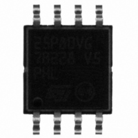
M25P80-VMW6TG NUMONYX, M25P80-VMW6TG Datasheet - Page 31

M25P80-VMW6TG
Manufacturer Part Number
M25P80-VMW6TG
Description
IC FLASH 8MBIT 75MHZ 8SOIC
Manufacturer
NUMONYX
Series
Forté™r
Datasheet
1.M25P80-VMP6G.pdf
(57 pages)
Specifications of M25P80-VMW6TG
Format - Memory
FLASH
Memory Type
FLASH
Memory Size
8M (1M x 8)
Speed
75MHz
Interface
SPI, 3-Wire Serial
Voltage - Supply
2.7 V ~ 3.6 V
Operating Temperature
-40°C ~ 85°C
Package / Case
8-SOIC (5.3mm Width), 8-SOP, 8-SOEIAJ
Package
8SO W
Cell Type
NOR
Density
8 Mb
Architecture
Sectored
Block Organization
Symmetrical
Typical Operating Supply Voltage
3.3 V
Sector Size
64KByte x 16
Timing Type
Synchronous
Interface Type
Serial-SPI
Access Time (max)
8ns
Boot Type
Not Required
Address Bus
1b
Operating Supply Voltage (typ)
3.3V
Operating Temp Range
-40C to 85C
Package Type
SOIC W
Program/erase Volt (typ)
2.7 to 3.6V
Sync/async
Synchronous
Operating Temperature Classification
Industrial
Operating Supply Voltage (min)
2.7V
Operating Supply Voltage (max)
3.6V
Word Size
8b
Number Of Words
1M
Supply Current
8mA
Mounting
Surface Mount
Pin Count
8
Lead Free Status / RoHS Status
Lead free / RoHS Compliant
Lead Free Status / RoHS Status
Lead free / RoHS Compliant
Other names
M25P80-VMW6TG
M25P80-VMW6TGTR
M25P80-VMW6TGTR
Available stocks
Company
Part Number
Manufacturer
Quantity
Price
Company:
Part Number:
M25P80-VMW6TG
Manufacturer:
MICRON
Quantity:
12 500
Company:
Part Number:
M25P80-VMW6TG
Manufacturer:
Numonyx
Quantity:
24 000
Company:
Part Number:
M25P80-VMW6TG
Manufacturer:
MICRON44
Quantity:
7 285
Part Number:
M25P80-VMW6TG
Manufacturer:
MICRON
Quantity:
20 000
Company:
Part Number:
M25P80-VMW6TG-N
Manufacturer:
STMicroelectronics
Quantity:
1
Part Number:
M25P80-VMW6TGBA
Manufacturer:
ST
Quantity:
20 000
6.9
Sector Erase (SE)
The Sector Erase (SE) instruction sets to 1 (FFh) all bits inside the chosen sector. Before it
can be accepted, a Write Enable (WREN) instruction must previously have been executed.
After the Write Enable (WREN) instruction has been decoded, the device sets the Write
Enable Latch (WEL).
The Sector Erase (SE) instruction is entered by driving Chip Select (S) Low, followed by the
instruction code, and three address bytes on Serial Data Input (D). Any address inside the
Sector (see
must be driven Low for the entire duration of the sequence.
The instruction sequence is shown in
Chip Select (S) must be driven High after the eighth bit of the last address byte has been
latched in, otherwise the Sector Erase (SE) instruction is not executed. As soon as Chip
Select (S) is driven High, the self-timed Sector Erase cycle (whose duration is t
initiated. While the Sector Erase cycle is in progress, the Status Register may be read to
check the value of the Write In Progress (WIP) bit. The Write In Progress (WIP) bit is 1
during the self-timed Sector Erase cycle, and is 0 when it is completed. At some unspecified
time before the cycle is completed, the Write Enable Latch (WEL) bit is reset.
A Sector Erase (SE) instruction applied to a page which is protected by the Block Protect
(BP2, BP1, BP0) bits (see
Figure 15. Sector Erase (SE) instruction sequence
1. Address bits A23 to A20 are Don’t Care.
S
C
D
Table
3) is a valid address for the Sector Erase (SE) instruction. Chip Select (S)
0
Table 3
1
2
Instruction
3
and
4
Figure
5
Table
6
7
15.
MSB
2) is not executed.
23 22
8
9
24 Bit Address
2
29 30 31
1
0
AI03751D
SE
) is
31/57


