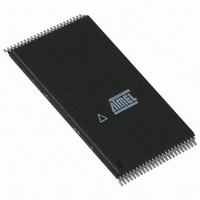
AT49BV8192A-90TC Atmel, AT49BV8192A-90TC Datasheet - Page 4

AT49BV8192A-90TC
Manufacturer Part Number
AT49BV8192A-90TC
Description
IC FLASH 8MBIT 90NS 48TSOP
Manufacturer
Atmel
Datasheet
1.AT49BV8192A-11CI.pdf
(20 pages)
Specifications of AT49BV8192A-90TC
Format - Memory
FLASH
Memory Type
FLASH
Memory Size
8M (1M x 8 or 512K x 16)
Speed
90ns
Interface
Parallel
Voltage - Supply
2.7 V ~ 3.6 V
Operating Temperature
0°C ~ 70°C
Package / Case
48-TSOP
Lead Free Status / RoHS Status
Contains lead / RoHS non-compliant
Other names
AT49BV8192A90TC
Device Operation
READ: The AT49BV/LV008A(T)/8192A(T) is accessed like an EPROM. When CE and
OE are low and WE is high, the data stored at the memory location determined by the
address pins is asserted on the outputs. The outputs are put in the high-impedance
state whenever CE or OE is high. This dual-line control gives designers flexibility in pre-
venting bus contention.
COMMAND SEQUENCES: When the device is first powered on it will be reset to the
read or standby mode depending upon the state of the control line inputs. In order to
perform other device functions, a series of command sequences are entered into the
device. The command sequences are shown in the Command Definitions table (I/O8 -
I/O15 are don’t care inputs for the command codes). The command sequences are writ-
ten by applying a low pulse on the WE or CE input with CE or WE low (respectively) and
OE high. The address is latched on the falling edge of CE or WE, whichever occurs last.
The data is latched by the first rising edge of CE or WE. Standard microprocessor write
timings are used. The address locations used in the command sequences are not
affected by entering the command sequences.
RESET: A RESET input pin is provided to ease some system applications. When
RESET is at a logic high level, the device is in its standard operating mode. A low level
on the RESET input halts the present device operation and puts the outputs of the
device in a high-impedance state. When a high level is reasserted on the RESET pin,
the device returns to the read or standby mode, depending upon the state of the control
inputs. By applying a 12V ± 0.5V input signal to the RESET pin the boot block array can
be reprogrammed even if the boot block program lockout feature has been enabled (see
Boot Block Programming Lockout Override section).
ERASURE: Before a byte or word can be reprogrammed, it must be erased. The erased
state of memory bits is a logic “1”. The entire device can be erased by using the Chip
Erase command or individual sectors can be erased by using the Sector Erase
commands.
CHIP ERASE: The entire device can be erased at one time by using the 6-byte chip
erase software code. After the chip erase has been initiated, the device will internally
time the erase operation so that no external clocks are required. The maximum time to
erase the chip is t
.
EC
If the boot block lockout has been enabled, the chip erase will not erase the data in the
boot block; it will erase the main memory block and the parameter blocks only. After the
chip erase, the device will return to the read or standby mode.
SECTOR ERASE: As an alternative to a full chip erase, the device is organized into four
sectors that can be individually erased. There are two 4K word parameter block sec-
tions, one boot block, and the main memory array block. The Sector Erase command is
a six-bus cycle operation. The sector address is latched on the falling WE edge of the
sixth cycle while the 30H data input command is latched at the rising edge of WE. The
sector erase starts after the rising edge of WE of the sixth cycle. The erase operation is
internally controlled; it will automatically time to completion. Whenever the main memory
block is erased and reprogrammed, the two parameter blocks should be erased and
reprogrammed before the main memory block is erased again. Whenever a parameter
block is erased and reprogrammed, the other parameter block should be erased and
reprogrammed before the first parameter block is erased again. Whenever the boot
block is erased and reprogrammed, the main memory block and the parameter block
should be erased and reprogrammed before the boot block is erased again.
BYTE/WORD PROGRAMMING: Once a memory block is erased, it is programmed (to
a logic “0”) on a byte-by-byte or word-by-word basis. Programming is accomplished via
AT49BV/LV008A(T)/8192A(T)
4
1049K–FLASH–11/02


