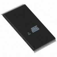
AT49BV8192A-90TC Atmel, AT49BV8192A-90TC Datasheet - Page 5

AT49BV8192A-90TC
Manufacturer Part Number
AT49BV8192A-90TC
Description
IC FLASH 8MBIT 90NS 48TSOP
Manufacturer
Atmel
Datasheet
1.AT49BV8192A-11CI.pdf
(20 pages)
Specifications of AT49BV8192A-90TC
Format - Memory
FLASH
Memory Type
FLASH
Memory Size
8M (1M x 8 or 512K x 16)
Speed
90ns
Interface
Parallel
Voltage - Supply
2.7 V ~ 3.6 V
Operating Temperature
0°C ~ 70°C
Package / Case
48-TSOP
Lead Free Status / RoHS Status
Contains lead / RoHS non-compliant
Other names
AT49BV8192A90TC
AT49BV/LV008A(T)/8192A(T)
the internal device command register and is a four-bus cycle operation. The device will
automatically generate the required internal program pulses.
Any commands written to the chip during the embedded programming cycle will be
ignored. If a hardware reset happens during programming, the data at the location being
programmed will be corrupted. Please note that a data “0” cannot be programmed back
to a “1”; only erase operations can convert “0”s to “1”s. Programming is completed after
the specified t
cycle time. The Data Polling feature may also be used to indicate the
BP
end of a program cycle.
BOOT BLOCK PROGRAMMING LOCKOUT: The device has one designated block
that has a programming lockout feature. This feature prevents programming of data in
the designated block once the feature has been enabled. The size of the block is 8K
words. This block, referred to as the boot block, can contain secure code that is used to
bring up the system. Enabling the lockout feature will allow the boot code to stay in the
device while data in the rest of the device is updated. This feature does not have to be
activated; the boot block’s usage as a write protected region is optional to the user. The
address range of the boot block is 00000H to 03FFFH for the AT49BV/LV008A; FC000H
to FFFFFH for the AT49BV/LV008AT; 00000H to 01FFFH for the AT49BV/LV8192A;
and 7E000H to 7FFFFH for the AT49BV/LV8192AT.
Once the feature is enabled, the data in the boot block can no longer be erased or pro-
grammed when input levels of 5.5V or less are used. Data in the main memory block
can still be changed through the regular programming method. To activate the lockout
feature, a series of six program commands to specific addresses with specific data must
be performed. Please refer to the Command Definitions table.
BOOT BLOCK LOCKOUT DETECTION: A software method is available to determine if
programming of the boot block section is locked out. When the device is in the software
product identification mode (see Software Product Identification Entry and Exit sections)
a read from the following address location will show if programming the boot block is
locked out – 00002H for the AT49BV/LV008A and AT49BV/LV8192A; FC002H for the
AT49BV/LV008AT; and 7E002H for the AT49BV/LV8192AT. If the data on I/O0 is low,
the boot block can be programmed; if the data on I/O0 is high, the program lockout fea-
ture has been enabled and the block cannot be programmed. The software product
identification exit code should be used to return to standard operation.
BOOT BLOCK PROGRAMMING LOCKOUT OVERRIDE: The user can override the
boot block programming lockout by taking the RESET pin to 12 volts during the entire
chip erase, sector erase or word programming operation. When the RESET pin is
brought back to TTL levels the boot block programming lockout feature is again active.
PRODUCT IDENTIFICATION: The product identification mode identifies the device and
manufacturer as Atmel. It may be accessed by hardware or software operation. The
hardware operation mode can be used by an external programmer to identify the correct
programming algorithm for the Atmel product.
For details, see “Operating Modes” on page 9 (for hardware operation) or “Software
Product Identification Entry/Exit” on page 15. The manufacturer and device code is the
same for both modes.
DATA POLLING: The AT49BV/LV008A(T)/8192A(T) features Data Polling to indicate
the end of a program cycle. During a program cycle an attempted read of the last byte
loaded will result in the complement of the loaded data on I/O7. Once the program cycle
has been completed, true data is valid on all outputs and the next cycle may begin. Dur-
ing a chip or sector erase operation, an attempt to read the device will give a “0” on I/O7.
Once the program or erase cycle has completed, true data will be read from the device.
Data Polling may begin at any time during the program cycle.
5
1049K–FLASH–11/02


