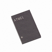
AT25P1024C1-10CI-2.7 Atmel, AT25P1024C1-10CI-2.7 Datasheet

AT25P1024C1-10CI-2.7
Specifications of AT25P1024C1-10CI-2.7
Available stocks
Related parts for AT25P1024C1-10CI-2.7
AT25P1024C1-10CI-2.7 Summary of contents
Page 1
... Description The AT25P1024 provides 1,048,576 bits of serial electrically erasable programmable read only memory (EEPROM) organized as 131,072 words of 8 bits each. The device is optimized for use in many industrial and commercial applications where low power and low voltage operation are essential. The AT25P1024 is available in space saving 20-lead JEDEC SOIC and 8-lead LAP packages ...
Page 2
Block Write protection is enabled by programming the status register with top ¼, top ½ or entire array of write protection. Separate Program Enable and Program Disable instructions are provided for additional data protection. Hardware data pro- tection is provided ...
Page 3
Table 2. Pin Capacitance Applicable over recommended operating range from T Symbol Test Conditions C Output Capacitance (SO) OUT C Input Capacitance (CS, SCK, SI, WP, HOLD) IN Note: 1. This parameter is characterized and is not 100% tested. ...
Page 4
Table 4. AC Characteristics Applicable over recommended operating range from TTL Gate and 100 pF (unless otherwise noted) L Symbol Parameter f SCK Clock Frequency SCK t Input Rise Time RI t Input Fall Time FI ...
Page 5
Serial Interface Description 1082I–SEEPR–7/06 MASTER: The device that generates the serial clock. SLAVE: Because the serial clock pin (SCK) is always an input, the AT25P1024 always operates as a slave. TRANSMITTER/RECEIVER: The AT25P1024 has separate pins designated for data transmission ...
Page 6
AT25P1024 6 Figure 2. SPI Serial Interface MASTER: MICROCONTROLLER DATA OUT (MOSI) DATA IN (MISO) SERIAL CLOCK (SPI CK) SLAVE: AT25P1024 SI SO SCK SS0 CS SS1 SI SS2 SO SS3 SCK SCK SCK ...
Page 7
... Table 6. Status Register Format Bit 7 Bit 6 Bit 5 WPEN X X AT25P1024 Operation Set Write Enable Latch Reset Write Enable Latch Read Status Register Write Status Register Read Data from Memory Array Write Data to Memory Array Bit 4 Bit 3 Bit 2 Bit 1 X BP1 BP0 WEN CC Bit 0 RDY 7 ...
Page 8
... WRITE STATUS REGISTER (WRSR): The WRSR instruction allows the user to select one of four levels of protection. The AT25P1024 is divided into four array segments. Top quarter (1/4), top half (1/2), or all of the memory segments can be protected. Any of the data within any selected segment will therefore be read only. The block write protection levels and corresponding status register control bits are shown in Table 8 ...
Page 9
... When the highest address is reached, the address counter will roll over to the lowest address allowing the entire memory to be read in one continuous read cycle. WRITE SEQUENCE (WRITE): In order to program the AT25P1024, two separate instructions must be executed ...
Page 10
Timing Diagrams (for SPI Mode 0 (0, 0)) Figure 3. Synchronous Data Timing CSS V IH SCK HI Figure 4. WREN Timing ...
Page 11
Figure 6. RDSR Timing CS 0 SCK SI HIGH IMPEDANCE SO Figure 7. WRSR Timing Figure 8. READ Timing SCK SI INSTRUCTION HIGH IMPEDANCE SO 1082I–SEEPR–7/ INSTRUCTION 7 ...
Page 12
Figure 9. WRITE Timing SCK SI INSTRUCTION HIGH IMPEDANCE SO Figure 10. HOLD Timing CS SCK HOLD SO AT25P1024 ...
Page 13
... Ordering Information Ordering Code AT25P1024C1-10CI-2.7 AT25P1024W1-10SI-2.7 (2) AT25P1024C1-10CU-2.7 (2) AT25P1024W1-10SU-2.7 Notes: 1. For 2.7V devices used in the 4.5V to 5.5V range, please refer to performance values in the AC and DC Characteristics tables. 2. “U” designates Green Package & RoHS Compliant. 8C1 8-pad, 0.300" Wide, Leadless Array Package (LAP) 20S2 20-lead, 0.300" ...
Page 14
Packaging Information 8C1 – LAP Marked Pin1 Indentifier E 0.10 mm TYP Bottom View Note: 1. Metal Pad Dimensions. 2. All exposed metal area shall have the following finished platings. Ni: 0.0005 to 0.015 ...
Page 15
JEDEC SOIC Top View e D Side View Notes: 1. This drawing is for general information only; refer to JEDEC Drawing MS-013, Variation AC for additional information. 2. Dimension "D" does not include mold Flash, protrusions or gate ...
Page 16
Revision History AT25P1024 16 Doc. Rev. Comments 1082I Added Note ‘Not Recommended for new design; please refer to AT25FS010 datasheet’ to first page. 1082I–SEEPR–7/06 ...
Page 17
... Disclaimer: The information in this document is provided in connection with Atmel products. No license, express or implied, by estoppel or otherwise, to any intellectual property right is granted by this document or in connection with the sale of Atmel products. EXCEPT AS SET FORTH IN ATMEL’S TERMS AND CONDI- TIONS OF SALE LOCATED ON ATMEL’S WEB SITE, ATMEL ASSUMES NO LIABILITY WHATSOEVER AND DISCLAIMS ANY EXPRESS, IMPLIED OR STATUTORY WARRANTY RELATING TO ITS PRODUCTS INCLUDING, BUT NOT LIMITED TO, THE IMPLIED WARRANTY OF MERCHANTABILITY, FITNESS FOR A PARTICULAR PURPOSE, OR NON-INFRINGEMENT ...


