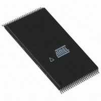
AT49BV160D-70TU Atmel, AT49BV160D-70TU Datasheet - Page 15

AT49BV160D-70TU
Manufacturer Part Number
AT49BV160D-70TU
Description
IC FLASH 16MBIT 70NS 48TSOP
Manufacturer
Atmel
Datasheet
1.AT49BV160D-70TU.pdf
(29 pages)
Specifications of AT49BV160D-70TU
Format - Memory
FLASH
Memory Type
FLASH
Memory Size
16M (1M x 16)
Speed
70ns
Interface
Parallel
Voltage - Supply
2.65 V ~ 3.6 V
Operating Temperature
-40°C ~ 85°C
Package / Case
48-TSOP
Lead Free Status / RoHS Status
Lead free / RoHS Compliant
Available stocks
Company
Part Number
Manufacturer
Quantity
Price
Company:
Part Number:
AT49BV160D-70TU
Manufacturer:
ATMEL
Quantity:
5 530
Company:
Part Number:
AT49BV160D-70TU
Manufacturer:
ATMEL
Quantity:
5 530
Part Number:
AT49BV160D-70TU
Manufacturer:
ATMEL/爱特梅尔
Quantity:
20 000
21. Command Definition Table
Notes:
22. Absolute Maximum Ratings*
3591C–FLASH–6/06
Command Sequence
Read
Sector Erase/Confirm
Word Program
Dual-word Program
Erase/Program Suspend
Erase/Program Resume
Product ID Entry
Sector Softlock
Sector Hardlock
Sector Unlock
Read Status Register
Clear Status Register
Program Protection Register
Lock Protection Register – Sector B
Status of Sector B Protection
CFI Query
Temperature under Bias ................................ -55°C to +125°C
Storage Temperature..................................... -65°C to +150°C
All Input Voltages
(including NC Pins)
with Respect to Ground ...................................-0.6V to +6.25V
All Output Voltages
with Respect to Ground ...........................-0.6V to V
Voltage on V
with Respect to Ground ...................................-0.6V to +10.0V
1. The DATA FORMAT shown for each bus cycle is as follows; I/O7 - I/O0 (Hex). I/O15 - I/O8 are don’t care. The ADDRESS
2. SA = sector address. Any word address within a sector can be used to designate the sector address (see pages
3. This fast programming option enables the user to program two words in parallel only when V
4. During the second bus cycle, the manufacturer code is read from address 00000H, the device code is read from address
5. The status register bits are output on I/O7 - I/O0.
6. Any addresses within the user programmable protection register region. Address locations are shown on
7. If data bit D1 is “0”, sector B is locked. If data bit D1 is “1”, sector B can be reprogrammed.
FORMAT shown for each bus cycle is as follows: A7 - A0 (Hex). Address A19 through A8 are don’t care.
for details).
Addr0 and Addr1, of the two words, D
manufacturing purposes only.
00001H, and the data in the protection register is read from addresses 00081H - 00088H.
ter Addressing Table” on page
PP
(4)
(3)
16.
Cycles
Bus
1
2
2
3
1
1
1
2
2
2
2
1
2
2
2
1
IN0
CCQ
and D
+ 0.6V
IN1
Addr
XX
XX
XX
XX
XX
XX
XX
XX
XX
XX
XX
XX
XX
XX
XX
XX
1st Bus Cycle
, must only differ in address A0. This command should be used during
*NOTICE:
40/10
Data
FF
E0
B0
D0
C0
C0
20
90
60
60
60
70
50
90
98
Stresses beyond those listed under “Absolute
Maximum Ratings” may cause permanent dam-
age to the device. This is a stress rating only and
functional operation of the device at these or any
other conditions beyond those indicated in the
operational sections of this specification is not
implied. Exposure to absolute maximum rating
conditions for extended periods may affect device
reliability.
Addr
Addr0
Addr
SA
SA
SA
SA
Addr
2nd Bus Cycle
XX
80
80
(2)
(2)
(2)
(2)
(6)
D
D
FFFD
Data
D
OUT
OUT
D
D
D0
D0
01
2F
AT49BV160D(T)
IN0
IN
IN
(5)
(7)
PP
= 9.5V. The addresses,
Addr1
Addr
3rd Bus Cycle
“Protection Regis-
17
Data
D
and
IN1
18
15


