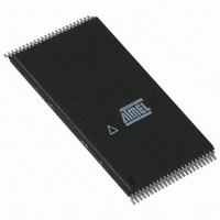
AT49BV160D-70TU Atmel, AT49BV160D-70TU Datasheet - Page 4

AT49BV160D-70TU
Manufacturer Part Number
AT49BV160D-70TU
Description
IC FLASH 16MBIT 70NS 48TSOP
Manufacturer
Atmel
Datasheet
1.AT49BV160D-70TU.pdf
(29 pages)
Specifications of AT49BV160D-70TU
Format - Memory
FLASH
Memory Type
FLASH
Memory Size
16M (1M x 16)
Speed
70ns
Interface
Parallel
Voltage - Supply
2.65 V ~ 3.6 V
Operating Temperature
-40°C ~ 85°C
Package / Case
48-TSOP
Lead Free Status / RoHS Status
Lead free / RoHS Compliant
Available stocks
Company
Part Number
Manufacturer
Quantity
Price
Company:
Part Number:
AT49BV160D-70TU
Manufacturer:
ATMEL
Quantity:
5 530
Company:
Part Number:
AT49BV160D-70TU
Manufacturer:
ATMEL
Quantity:
5 530
Part Number:
AT49BV160D-70TU
Manufacturer:
ATMEL/爱特梅尔
Quantity:
20 000
4.3
4.4
4.4.1
4.5
4.6
4
Reset
Erase
Word Programming
VPP Pin
AT49BV160D(T)
Sector Erase
A RESET input pin is provided to ease some system applications. When RESET is at a logic
high level, the device is in its standard operating mode. A low level on the RESET input halts the
present device operation and puts the outputs of the device in a high impedance state. When a
high level is reasserted on the RESET pin, the device returns to the read mode, depending upon
the state of the control inputs.
Before a word can be reprogrammed, it must be erased. The erased state of memory bits is a
logical “1”. The individual sectors can be erased by using the Sector Erase command.
The device is organized into 39 sectors (SA0 - SA38) that can be individually erased. The Sector
Erase command is a two-bus cycle operation. The sector address and the D0H Data Input com-
mand are latched on the rising edge of WE. The sector erase starts after the rising edge of WE
of the second cycle provided the given sector has not been protected. The erase operation is
internally controlled; it will automatically time to completion. The maximum time to erase a sector
is t
ing immediately.
Once a memory sector is erased, it is programmed (to a logical “0”) on a word-by-word basis.
Programming is accomplished via the Internal Device command register and is a two-bus cycle
operation. The device will automatically generate the required internal program pulses.
Any commands written to the chip during the embedded programming cycle will be ignored. If a
hardware reset happens during programming, the data at the location being programmed will be
corrupted. Please note that a data “0” cannot be programmed back to a “1”; only erase opera-
tions can convert “0”s to “1”s. Programming is completed after the specified t
program status bit is a “1”, the device was not able to verify that the program operation was per-
formed successfully. The status register indicates the programming status. While the program
sequence executes, status bit I/O7 is “0”. While programming, the only valid commands are
Read Status Register, Program Suspend and Program Resume.
The circuitry of the AT49BV160D(T) is designed so that the device cannot be programmed or
erased if the V
erase operations can be performed. The VPP pin cannot be left floating.
SEC
. An attempt to erase a sector that has been protected will result in the operation terminat-
PP
voltage is less that 0.4V. When V
PP
is at 1.65V or above, normal program and
BP
cycle time. If the
3591C–FLASH–6/06


