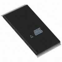
AT49BV160D-70TU Atmel, AT49BV160D-70TU Datasheet - Page 9

AT49BV160D-70TU
Manufacturer Part Number
AT49BV160D-70TU
Description
IC FLASH 16MBIT 70NS 48TSOP
Manufacturer
Atmel
Datasheet
1.AT49BV160D-70TU.pdf
(29 pages)
Specifications of AT49BV160D-70TU
Format - Memory
FLASH
Memory Type
FLASH
Memory Size
16M (1M x 16)
Speed
70ns
Interface
Parallel
Voltage - Supply
2.65 V ~ 3.6 V
Operating Temperature
-40°C ~ 85°C
Package / Case
48-TSOP
Lead Free Status / RoHS Status
Lead free / RoHS Compliant
Available stocks
Company
Part Number
Manufacturer
Quantity
Price
Company:
Part Number:
AT49BV160D-70TU
Manufacturer:
ATMEL
Quantity:
5 530
Company:
Part Number:
AT49BV160D-70TU
Manufacturer:
ATMEL
Quantity:
5 530
Part Number:
AT49BV160D-70TU
Manufacturer:
ATMEL/爱特梅尔
Quantity:
20 000
4.12
4.13
4.14
4.15
4.16
3591C–FLASH–6/06
128-bit Protection Register
Common Flash Interface (CFI)
Hardware Data Protection
Input Levels
Output Levels
The AT49BV160D(T) contains a 128-bit register that can be used for security purposes in sys-
tem design. The protection register is divided into two 64-bit sectors. The two sectors are
designated as sector A and sector B. The data in sector A is non-changeable and is pro-
grammed at the factory with a unique number. The data in sector B is programmed by the user
and can be locked out such that data in the sector cannot be reprogrammed. To program sector
B in the protection register, the two-bus cycle Program Protection Register command must be
used as shown in the
cycle Lock Protection Register command must be used as shown in the
Table”
ond bus cycle are don’t cares. To determine whether sector B is locked out, use the status of
sector B protection command. If data bit D1 is zero, sector B is locked. If data bit D1 is one, sec-
tor B can be reprogrammed. Please see the
for the address locations in the protection register. To read the protection register, the Product
ID Entry command is given followed by a normal read operation from an address within the pro-
tection register. After determining whether sector B is protected or not, or reading the protection
register, the Read command must be given to return to the read mode.
CFI is a published, standardized data structure that may be read from a flash device. CFI allows
system software to query the installed device to determine the configurations, various electrical
and timing parameters and functions supported by the device. CFI is used to allow the system to
learn how to interface to the flash device most optimally. The two primary benefits of using CFI
are ease of upgrading and second source availability. The command to enter the CFI Query
mode is a one-bus cycle command which requires writing data 98h to any address. The CFI
Query command can be written when the device is ready to read data or can also be written
when the part is in the product ID mode. Once in the CFI Query mode, the system can read CFI
data at the addresses given in
to the read mode, issue the Read command.
The Hardware Data Protection feature protects against inadvertent programs to the
AT49BV160D(T) in the following ways: (a) V
function is inhibited. (b) Program inhibit: holding any one of OE low, CE high or WE high inhibits
program cycles. (c) Program inhibit: V
While operating with a 2.65V to 3.6V power supply, the address inputs and control inputs (OE,
CE and WE) may be driven from 0 to 5.5V without adversely affecting the operation of the
device. The I/O lines can only be driven from 0 to V
For the AT49BV160D(T), output high levels (V
2.65V -3.6V output levels, V
. Data bit D1 must be zero during the second bus cycle. All other data bits during the sec-
“Command Definition Table” on page
CCQ
“Common Flash Interface Definition Table” on page
must be tied to V
PP
is less than V
CC
“Protection Register Addressing Table” on page 16
sense: if V
CC
OH
CCQ
.
) are equal to V
ILPP
+ 0.6V.
CC
.
15. To lock out sector B, the two-bus
is below 1.8V (typical), the program
AT49BV160D(T)
CCQ
- 0.1V (not V
“Command Definition
24. To return
CC
). For
9


