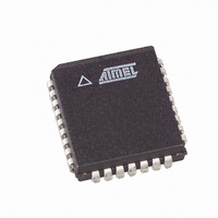
AT49LH00B4-33JX Atmel, AT49LH00B4-33JX Datasheet - Page 10

AT49LH00B4-33JX
Manufacturer Part Number
AT49LH00B4-33JX
Description
IC FLASH 4MBIT 33MHZ 32PLCC
Manufacturer
Atmel
Datasheet
1.AT49LH00B4-33JC.pdf
(41 pages)
Specifications of AT49LH00B4-33JX
Format - Memory
FLASH
Memory Type
FLASH
Memory Size
4M (512K x 8)
Speed
33MHz
Interface
Parallel
Voltage - Supply
3 V ~ 3.6 V
Operating Temperature
0°C ~ 85°C
Package / Case
32-PLCC
Lead Free Status / RoHS Status
Lead free / RoHS Compliant
Available stocks
Company
Part Number
Manufacturer
Quantity
Price
Part Number:
AT49LH00B4-33JX
Manufacturer:
AT
Quantity:
20 000
7.3.7
7.4
Figure 7-2.
10
FWH4/LFRAME
FWH/LAD[3:0]
FWH Read Cycle
CLK
AT49LH00B4
SYNC (Synchronize) Field
FWH Read Cycle
1101b
START
1
IDSEL
IDSEL
2
This field is used to add wait-states for an access. It can be several clocks in length. On target
cycles, this field is driven by the FWH memory device. If the FWH device needs to assert wait-
states, it does so by driving a “wait” SYNC value of 0101b on the FWH/LAD[3:0] pins until it is
ready. When ready, the device will drive a “ready” SYNC value of 0000b on the FWH/LAD[3:0]
lines. Valid values for the SYNC field are shown in
Table 7-2.
FWH read cycles are used to read data from the memory array, the Sector Locking Registers,
the GPI register, the Status Register, and to read the product ID information. Upon initial device
power-up or after exiting from a reset condition, the device will automatically default to the read
array mode.
Valid FWH read cycles begin with a START field of 1101b being sent to the device. Following
the IDSEL, MADDR, and MSIZE fields, a 2-clock TAR field must be sent to the device to indicate
that the master is turning control of the LPC bus over to the FWH memory device. After the sec-
ond clock of the TAR phase, the FWH device assumes control of the bus and begins driving
SYNC fields to add wait-states. When the device is ready to output data, it will first send a
“ready” SYNC and then output one byte of data during the next two clock cycles. The data is
sent one nibble at a time with the low nibble being output first followed by the high nibble. After
the data has been output, the FWH device will send a 2-clock TAR field to the master to indicate
that it is turning control of the LPC bus back over to the master.
Table 7-2
memory array.
SYNC Value
0000b
0101b
A27-A24 A23-A20 A19-A16
3
shows a FWH read cycle that requires three SYNC clocks to access data from the
4
Valid SYNC Values
5
A15-A12
MADDR
6
SYNC Type
RSYNC (Ready SYNC) – Synchronization has been achieved with no error.
WSYNC (Wait SYNC) – Device is indicating wait-states (also referred to as
short-sync).
A11-A8
7
A7-A4
8
A3-A0
9
0000b
MSIZE
10
1111b
TAR0
11
High-Z
Table
TAR1
12
WSYNC
0101b
7-2.
13
WSYNC
0101b
14
RSYNC
0000b
15
D3-D0
DATA
16
D7-D4
DATA
17
3379C–FLASH–3/05
1111b
TAR0
18
High-Z
TAR1
19


