AT45DB321C-TC Atmel, AT45DB321C-TC Datasheet - Page 7
AT45DB321C-TC
Manufacturer Part Number
AT45DB321C-TC
Description
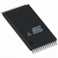
IC FLASH 32MBIT 40MHZ 28TSOP
Manufacturer
Atmel
Datasheet
1.AT45DB321C-RU.pdf
(40 pages)
Specifications of AT45DB321C-TC
Format - Memory
FLASH
Memory Type
DataFLASH
Memory Size
32M (8192 pages x 528 bytes)
Speed
40MHz
Interface
SPI, 3-Wire Serial
Voltage - Supply
2.7 V ~ 3.6 V
Operating Temperature
0°C ~ 70°C
Package / Case
28-TSOP
Lead Free Status / RoHS Status
Contains lead / RoHS non-compliant


Table 5-1.
5.2.6
5.3
5.3.1
3387M–DFLASH–2/08
PA12
0
0
0
0
1
1
1
1
•
•
•
Additional Commands
PA11
Main Memory Page Program Through Buffer
Main Memory Page to Buffer Transfer
0
0
0
0
1
1
1
1
•
•
•
Block Erase Addressing
PA10
0
0
0
0
1
1
1
1
•
•
•
This operation is a combination of the Buffer Write and Buffer to Main Memory Page Program
with Built-in Erase operations. Data is first clocked into buffer 1 or buffer 2 from the input pin (SI)
and then programmed into a specified page in the main memory. To initiate the operation, an
8-bit opcode, 82H for buffer 1 or 85H for buffer 2, must first be clocked into the device, followed
by three address bytes. The address bytes are comprised of one reserved bit, 13 page address
bits (PA12-PA0) that select the page in the main memory where data is to be written, and
10 buffer address bits (BFA9-BFA0) that select the first byte in the buffer to be written. After all
address bytes are clocked in, the part will take data from the input pins and store it in the speci-
fied data buffer. If the end of the buffer is reached, the device will wrap around back to the
beginning of the buffer. When there is a low-to-high transition on the CS pin, the part will first
erase the selected page in main memory to all 1s and then program the data stored in the buffer
into that memory page. Both the erase and the programming of the page are internally self-timed
and should take place in a maximum time of t
RDY/BUSY pin will indicate that the part is busy.
A page of data can be transferred from the main memory to either buffer 1 or buffer 2. To start
the operation, a 1-byte opcode, 53H for buffer 1 and 55H for buffer 2, must be clocked into the
device, followed by three address bytes comprised of one reserved bit, 13 page address bits
(PA12- PA0), which specify the page in main memory that is to be transferred, and 10 don’t care
bits. The CS pin must be low while toggling the SCK pin to load the opcode and the address
bytes from the input pin (SI). The transfer of the page of data from the main memory to the buffer
will begin when the CS pin transitions from a low to a high state. During the transfer of a page of
data (t
pleted or not.
PA9
0
0
0
0
1
1
1
1
•
•
•
XFR
), the status register can be read to determine whether the transfer has been com-
PA8
0
0
0
0
1
1
1
1
•
•
•
PA7
0
0
0
0
1
1
1
1
•
•
•
PA6
0
0
0
0
1
1
1
1
•
•
•
PA5
0
0
0
0
1
1
1
1
•
•
•
PA4
0
0
1
1
0
0
1
1
•
•
•
EP
. During this time, the status register and the
PA3
0
1
0
1
0
1
0
1
•
•
•
PA2
X
X
X
X
X
X
X
X
•
•
•
AT45DB321C
PA1
X
X
X
X
X
X
X
X
•
•
•
PA0
X
X
X
X
X
X
X
X
•
•
•
Block
1020
1021
1022
1023
0
1
2
3
•
•
•
7
Related parts for AT45DB321C-TC
Image
Part Number
Description
Manufacturer
Datasheet
Request
R

Part Number:
Description:
DEV KIT FOR AVR/AVR32
Manufacturer:
Atmel
Datasheet:

Part Number:
Description:
INTERVAL AND WIPE/WASH WIPER CONTROL IC WITH DELAY
Manufacturer:
ATMEL Corporation
Datasheet:
Part Number:
Description:
Low-Voltage Voice-Switched IC for Hands-Free Operation
Manufacturer:
ATMEL Corporation
Datasheet:
Part Number:
Description:
MONOLITHIC INTEGRATED FEATUREPHONE CIRCUIT
Manufacturer:
ATMEL Corporation
Datasheet:
Part Number:
Description:
AM-FM Receiver IC U4255BM-M
Manufacturer:
ATMEL Corporation
Datasheet:
Part Number:
Description:
Monolithic Integrated Feature Phone Circuit
Manufacturer:
ATMEL Corporation
Datasheet:
Part Number:
Description:
Multistandard Video-IF and Quasi Parallel Sound Processing
Manufacturer:
ATMEL Corporation
Datasheet:
Part Number:
Description:
High-performance EE PLD
Manufacturer:
ATMEL Corporation
Datasheet:
Part Number:
Description:
8-bit Flash Microcontroller
Manufacturer:
ATMEL Corporation
Datasheet:
Part Number:
Description:
2-Wire Serial EEPROM
Manufacturer:
ATMEL Corporation
Datasheet: