AT45DB041D-MU-2.5 Atmel, AT45DB041D-MU-2.5 Datasheet - Page 21
AT45DB041D-MU-2.5
Manufacturer Part Number
AT45DB041D-MU-2.5
Description
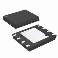
IC FLASH 4MBIT 66MHZ 8MLF
Manufacturer
Atmel
Datasheet
1.AT45DB041D-MU.pdf
(55 pages)
Specifications of AT45DB041D-MU-2.5
Format - Memory
FLASH
Memory Type
DataFLASH
Memory Size
4M (2048 pages x 264 bytes)
Speed
66MHz
Interface
SPI, RapidS
Voltage - Supply
2.5 V ~ 3.6 V
Operating Temperature
-40°C ~ 85°C
Package / Case
8-VFQFN, 8-VFQFPN
Architecture
Sectored
Interface Type
SPI
Supply Voltage (max)
3.6 V
Supply Voltage (min)
2.5 V
Maximum Operating Current
15 mA
Mounting Style
SMD/SMT
Organization
64 KB x 8
Density
4Mb
Access Time (max)
8ns
Boot Type
Not Required
Address Bus
1b
Operating Supply Voltage (typ)
3/3.3V
Operating Temp Range
-40C to 85C
Package Type
MLF
Program/erase Volt (typ)
2.5 to 3.6V
Sync/async
Synchronous
Operating Temperature Classification
Industrial
Operating Supply Voltage (min)
2.5V
Operating Supply Voltage (max)
3.6V
Supply Current
15mA
Mounting
Surface Mount
Pin Count
8
Lead Free Status / RoHS Status
Lead free / RoHS Compliant
Available stocks
Company
Part Number
Manufacturer
Quantity
Price
Company:

Part Number:
AT45DB041D-MU-2.5
Manufacturer:
ATMEL
Quantity:
1 600
Part Number:
AT45DB041D-MU-2.5
Manufacturer:
ATMEL/爱特梅尔
Quantity:
20 000


10.2.2
11. Additional Commands
11.1
11.2
3595P–DFLASH–09/09
Main Memory Page to Buffer Transfer
Main Memory Page to Buffer Compare
Reading the Security Register
The Security Register can be read by first asserting the CS pin and then clocking in an opcode
of 77H followed by three dummy bytes. After the last don't care bit has been clocked in, the con-
tent of the Security Register can be clocked out on the SO pins. After the last byte of the
Security Register has been read, additional pulses on the SCK pin will simply result in undefined
data being output on the SO pins.
Deasserting the CS pin will terminate the Read Security Register operation and put the SO pins
into a high-impedance state.
Figure 10-4. Read Security Register
A page of data can be transferred from the main memory to either buffer 1 or buffer 2. To start
the operation for the DataFlash standard page size (264 bytes), a 1-byte opcode, 53H for buffer
1 and 55H for buffer 2, must be clocked into the device, followed by three address bytes com-
prised of 4 don’t care bits, 11 page address bits (PA10 - PA0), which specify the page in main
memory that is to be transferred, and 9 don’t care bits. To perform a main memory page to buffer
transfer for the binary page size (256 bytes), the opcode 53H for buffer 1 or 55H for buffer 2,
must be clocked into the device followed by three address bytes consisting of 5 don’t care bits,
11 page address bits (A18 - A8) which specify the page in the main memory that is to be trans-
ferred, and 8 don’t care bits. The CS pin must be low while toggling the SCK pin to load the
opcode and the address bytes from the input pin (SI). The transfer of the page of data from the
main memory to the buffer will begin when the CS pin transitions from a low to a high state. Dur-
ing the transfer of a page of data (t
transfer has been completed.
A page of data in main memory can be compared to the data in buffer 1 or buffer 2. To initiate
the operation for the DataFlash standard page size, a 1-byte opcode, 60H for buffer 1 and 61H
for buffer 2, must be clocked into the device, followed by three address bytes consisting of
4 don’t care bits, 11 page address bits (PA10 - PA0) that specify the page in the main memory
that is to be compared to the buffer, and 9 don’t care bits. To start a main memory page to buffer
compare for a binary page size, the opcode 60H for buffer 1 or 61H for buffer 2, must be clocked
into the device followed by three address bytes consisting of 5 don’t care bits, 11 page address
bits (A18 - A8) that specify the page in the main memory that is to be compared to the buffer,
and 8 don’t care bits. The CS pin must be low while toggling the SCK pin to load the opcode and
CS
SO
SI
Each transition
represents 8 bits
Opcode
X
XFR
), the status register can be read to determine whether the
X
X
Data Byte
n
Data Byte
n + 1
AT45DB041D
Data Byte
n + x
21
Related parts for AT45DB041D-MU-2.5
Image
Part Number
Description
Manufacturer
Datasheet
Request
R

Part Number:
Description:
IC FLASH 4MBIT 66MHZ 8MLF
Manufacturer:
Atmel
Datasheet:

Part Number:
Description:
IC FLASH 4MBIT 66MHZ 8SOIC
Manufacturer:
Atmel
Datasheet:
Part Number:
Description:
IC FLASH 4MBIT 66MHZ 8SOIC
Manufacturer:
Atmel
Datasheet:
Part Number:
Description:
IC FLASH 4MBIT 66MHZ 8SOIC
Manufacturer:
Atmel
Datasheet:

Part Number:
Description:
At45db041d 4-megabit 2.5-volt Or 2.7-volt Dataflash
Manufacturer:
ATMEL Corporation
Datasheet:

Part Number:
Description:
Manufacturer:
Atmel
Datasheet:
Part Number:
Description:
Manufacturer:
ATMEL Corporation
Datasheet:
Part Number:
Description:
Manufacturer:
ATMEL Corporation
Datasheet:
Part Number:
Description:
Manufacturer:
ATMEL Corporation
Datasheet:
Part Number:
Description:
Manufacturer:
ATMEL Corporation
Datasheet:
Part Number:
Description:
Manufacturer:
ATMEL Corporation
Datasheet: