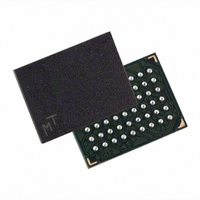
MT45W4MW16BCGB-701 WT Micron Technology Inc, MT45W4MW16BCGB-701 WT Datasheet - Page 27

MT45W4MW16BCGB-701 WT
Manufacturer Part Number
MT45W4MW16BCGB-701 WT
Description
IC PSRAM 64MBIT 70NS 54VFBGA
Manufacturer
Micron Technology Inc
Datasheet
1.MT45W4MW16BCGB-701_IT.pdf
(69 pages)
Specifications of MT45W4MW16BCGB-701 WT
Format - Memory
RAM
Memory Type
PSRAM (Page)
Memory Size
64M (4M x 16)
Speed
70ns
Interface
Parallel
Voltage - Supply
1.7 V ~ 1.95 V
Operating Temperature
-30°C ~ 85°C
Package / Case
54-VFBGA
Operating Temperature (max)
85C
Mounting
Surface Mount
Operating Temperature Classification
Commercial
Lead Free Status / RoHS Status
Lead free / RoHS Compliant
Drive Strength (BCR[5:4]) Default = Outputs Use Half-Drive Strength
Table 5:
WAIT Configuration (BCR[8]) Default = WAIT Transitions One Clock Before Data Valid/Invalid
WAIT Polarity (BCR[10]) Default = WAIT Active HIGH
Figure 19:
PDF: 09005aef8247bd51/Source: 09005aef8247bd83
64mb_burst_cr1_5_p25z_133mhz__2.fm - Rev. F 9/07 EN
BCR[5]
0
0
1
1
Drive Strength
WAIT Configuration (BCR[8] = 0)
BCR[4]
0
1
0
1
Note:
The output driver strength can be altered to full, one-half, or one-quarter strength to
adjust for different data bus loading scenarios. The reduced-strength options are
intended for stacked chip (Flash + CellularRAM) environments when there is a dedicated
memory bus. The reduced-drive-strength option minimizes the noise generated on the
data bus during READ operations. Full output drive strength should be selected when
using a discrete CellularRAM device in a more heavily loaded data bus environment.
Outputs are configured at half-drive strength during testing. See Table 5 for additional
information.
The WAIT configuration bit is used to determine when WAIT transitions between the
asserted and the de-asserted state with respect to valid data presented on the data bus.
The memory controller will use the WAIT signal to coordinate data transfer during
synchronous READ and WRITE operations. When BCR[8] = 0, data will be valid or invalid
on the clock edge immediately after WAIT transitions to the de-asserted or asserted
state, respectively (see Figures 19 and 21). When A8 = 1, the WAIT signal transitions one
clock period prior to the data bus going valid or invalid (see Figure 20 on page 28 and
Figure 21 on page 28).
The WAIT polarity bit indicates whether an asserted WAIT output should be HIGH or
LOW. This bit will determine whether the WAIT signal requires a pull-up or pull-down
resistor to maintain the de-asserted state.
DQ[15:0]
WAIT
Drive Strength
Data valid/invalid immediately after WAIT transitions (BCR[8] = 0). See Figure 21 on
page 28.
CLK
1/2 (default)
64Mb: 4 Meg x 16 Async/Page/Burst CellularRAM 1.5 Memory
Full
1/4
High-Z
Data 0
Impedance Typ (Ω) Use Recommendation
Data 1
25–30
27
100
50
Micron Technology, Inc., reserves the right to change products or specifications without notice.
Reserved
CL = 30pF to 50pF
CL = 15pF to 30pF, 104 MHz at light load
CL = 15pF or lower
©2005 Micron Technology, Inc. All rights reserved.
Registers


