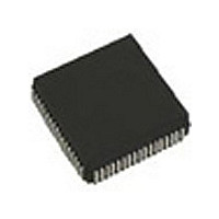
CY7C138-25JC Cypress Semiconductor Corp, CY7C138-25JC Datasheet - Page 6

CY7C138-25JC
Manufacturer Part Number
CY7C138-25JC
Description
IC SRAM 32KBIT 25NS 68PLCC
Manufacturer
Cypress Semiconductor Corp
Specifications of CY7C138-25JC
Format - Memory
RAM
Memory Type
SRAM - Dual Port, Asynchronous
Memory Size
32K (4K x 8)
Speed
25ns
Interface
Parallel
Voltage - Supply
4.5 V ~ 5.5 V
Operating Temperature
0°C ~ 70°C
Package / Case
68-PLCC
Density
32Kb
Access Time (max)
25ns
Sync/async
Asynchronous
Architecture
Not Required
Clock Freq (max)
Not RequiredMHz
Operating Supply Voltage (typ)
5V
Address Bus
12b
Package Type
PLCC
Operating Temp Range
0C to 70C
Number Of Ports
2
Supply Current
180mA
Operating Supply Voltage (min)
4.5V
Operating Supply Voltage (max)
5.5V
Operating Temperature Classification
Commercial
Mounting
Surface Mount
Pin Count
68
Word Size
8b
Number Of Words
4K
Lead Free Status / RoHS Status
Contains lead / RoHS non-compliant
Other names
428-1445
Available stocks
Company
Part Number
Manufacturer
Quantity
Price
Company:
Part Number:
CY7C138-25JC
Manufacturer:
CYPRESS
Quantity:
13 888
Company:
Part Number:
CY7C138-25JC
Manufacturer:
Cypress Semiconductor Corp
Quantity:
10 000
Switching Characteristics
Switching Waveforms
Notes
Document #: 38-06037 Rev. *E
t
t
t
t
t
t
t
t
t
t
t
t
t
t
t
t
t
9. Test conditions assume signal transition time of 3 ns or less, timing reference levels of 1.5V, input pulse levels of 0 to 3.0V, and output loading of the specified I
10. At any temperature and voltage condition for any device, t
11. Test conditions used are Load 3.
12. This parameter is guaranteed but not tested.
13. For information on part-to-part delay through RAM cells from writing port to reading port, refer to Read Timing with Port-to-Port Delay waveform.
14. Test conditions used are Load 2.
15. t
HZWE
LZWE
WDD
DDD
BLA
BHA
BLC
BHC
PS
WB
WH
BDD
INS
INR
SOP
SWRD
SPS
BUSY TIMING
INTERRUPT TIMING
SEMAPHORE TIMING
Parameter
and 30-pF load capacitance.
BDD
DATA OUT
ADDRESS
[15]
[13]
[13]
[11,12]
[11,12]
is a calculated parameter and is the greater of t
R/W LOW to High Z
R/W HIGH to Low Z
Write Pulse to Data Delay
Write Data Valid to Read Data Valid
BUSY LOW from Address Match
BUSY HIGH from Address Mismatch
BUSY LOW from CE LOW
BUSY HIGH from CE HIGH
Port Setup for Priority
R/W LOW after BUSY LOW
R/W HIGH after BUSY HIGH
BUSY HIGH to Data Valid
INT Set Time
INT Reset Time
SEM Flag Update Pulse (OE or SEM)
SEM Flag Write to Read Time
SEM Flag Contention Window
[14]
PREVIOUS DATA VALID
[14]
Description
t
OHA
Figure 3. Read Cycle No. 1 (Either Port Address Access)
Over the Operating Range
t
WDD
AA
– t
HZCE
PWE
is less than t
(actual) or t
Min
13
10
3
5
0
5
5
7C138-15
7C139-15
LZCE
DDD
Note 15
t
RC
[9]
Max
10
30
25
15
15
15
15
15
15
– t
and t
(continued)
SD
HZOE
(actual).
Min
20
10
3
5
0
5
5
is less than t
7C138-25
7C139-25
Note 15
Max
15
50
30
20
20
20
20
25
25
LZOE
.
Min
DATA VALID
30
15
3
5
0
5
5
7C138-35
7C139-35
[16, 17]
Note 15
CY7C138, CY7C139
Max
20
60
35
20
20
20
20
25
25
Min
40
20
3
5
0
5
5
7C138-55
7C139-55
Note 15
Max
25
70
40
45
40
40
35
30
30
Page 6 of 17
Unit
OI
ns
ns
ns
ns
ns
ns
ns
ns
ns
ns
ns
ns
ns
ns
ns
ns
ns
/I
OH
[+] Feedback


