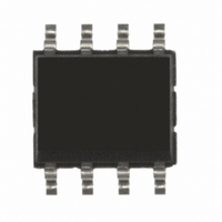
M25P40-VMN6P NUMONYX, M25P40-VMN6P Datasheet - Page 41

M25P40-VMN6P
Manufacturer Part Number
M25P40-VMN6P
Description
IC FLASH 4MBIT 50MHZ 8SOIC
Manufacturer
NUMONYX
Series
Forté™r
Specifications of M25P40-VMN6P
Format - Memory
FLASH
Memory Type
FLASH
Memory Size
4M (512K x 8)
Speed
50MHz
Interface
SPI, 3-Wire Serial
Voltage - Supply
2.3 V ~ 3.6 V
Operating Temperature
-40°C ~ 85°C
Package / Case
8-SOIC (3.9mm Width)
Memory Configuration
512K X 8
Ic Interface Type
Serial, SPI
Clock Frequency
50MHz
Supply Voltage Range
2.3V To 3.6V
Memory Case Style
SOIC
No. Of Pins
8
Lead Free Status / RoHS Status
Lead free / RoHS Compliant
Other names
497-3598
497-3598
497-3598
Available stocks
Company
Part Number
Manufacturer
Quantity
Price
Part Number:
M25P40-VMN6P
Manufacturer:
ST
Quantity:
20 000
Company:
Part Number:
M25P40-VMN6PB
Manufacturer:
ST
Quantity:
102
Part Number:
M25P40-VMN6PB
Manufacturer:
ST
Quantity:
20 000
Part Number:
M25P40-VMN6PBA
Manufacturer:
MICRON
Quantity:
20 000
Table 16.
1. t
2. Value guaranteed by characterization, not 100% tested in production.
3. Expressed as a slew-rate.
4. Only applicable as a constraint for a WRSR instruction when SRWD is set at ‘1’.
Symbol
t
t
t
t
t
t
t
t
t
HHQX
WHSL
SHWL
CLCH
CHCL
SHQZ
HLQZ
RES1
RES2
t
t
t
t
t
t
t
t
t
t
t
t
t
t
t
t
DVCH
CHDX
CHSH
SHCH
CHHH
HHCH
t
CH
SLCH
CHSL
CLQV
CLQX
HLCH
CHHL
CL
SHSL
DP
W
CH
f
f
C
R
(5)
(1)
(1)
(2)
+ t
(2)
(2)
(2)
(2)
(2)
(2)
(2)
(4)
(4)
CL
must be greater than or equal to 1/ f
t
t
t
t
t
Alt.
t
t
t
CLH
CSS
DSU
CSH
t
CLL
t
DIS
HO
f
DH
t
AC characteristics (25 MHz operation)
HZ
LZ
C
V
Clock frequency for the following instructions:
FAST_READ, PP, SE, BE, DP, RES, WREN,
WRDI, RDSR, WRSR
Clock frequency for READ instructions
Clock High time
Clock Low time
Clock Rise time
Clock Fall time
S Active Setup time (relative to C)
S Not Active Hold time (relative to C)
Data In Setup time
Data In Hold time
S Active Hold time (relative to C)
S Not Active Setup time (relative to C)
S Deselect time
Output Disable time
Clock Low to Output Valid
Output Hold time
HOLD Setup time (relative to C)
HOLD Hold time (relative to C)
HOLD Setup time (relative to C)
HOLD Hold time (relative to C)
HOLD to Output Low-Z
HOLD to Output High-Z
Write Protect Setup time
Write Protect Hold time
S High to Deep Power-down mode
S High to Standby mode without Electronic
Signature Read
S High to Standby mode with Electronic
Signature Read
Write Status Register cycle time
Test conditions specified in
(3)
(3)
Parameter
(peak to peak)
(peak to peak)
C
.
Table 10
—
—
—
—
—
—
Min
100
100
DC
DC
0.1
0.1
18
18
10
10
10
10
10
10
10
10
20
and
5
5
0
Table 12
—
—
—
—
—
—
—
—
—
—
—
—
—
—
—
—
—
—
—
—
—
—
—
—
—
—
—
Typ
1.5
—
—
—
—
—
—
—
—
—
—
—
—
—
—
—
—
—
—
Max
1.8
25
20
15
15
15
20
15
3
3
MHz
MHz
V/ns
V/ns
Unit
ms
41/59
ns
ns
ns
ns
ns
ns
ns
ns
ns
ns
ns
ns
ns
ns
ns
ns
ns
ns
ns
ns
µs
µs
µs


