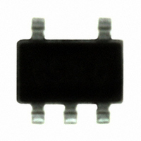
JS28F320C3TD70 NUMONYX, JS28F320C3TD70 Datasheet - Page 23

JS28F320C3TD70
Manufacturer Part Number
JS28F320C3TD70
Description
IC FLASH 32MBIT 70NS 48TSOP
Manufacturer
NUMONYX
Datasheet
1.JS28F320C3BD70A.pdf
(68 pages)
Specifications of JS28F320C3TD70
Format - Memory
FLASH
Memory Type
Advanced + Boot Block FLASH
Memory Size
32M (2M x 16)
Speed
70ns
Interface
Parallel
Voltage - Supply
2.7 V ~ 3.6 V
Operating Temperature
-40°C ~ 85°C
Package / Case
48-TSOP
Lead Free Status / RoHS Status
Lead free / RoHS Compliant
Other names
864838
Available stocks
Company
Part Number
Manufacturer
Quantity
Price
Company:
Part Number:
JS28F320C3TD70
Manufacturer:
INTEL
Quantity:
5 530
Company:
Part Number:
JS28F320C3TD70
Manufacturer:
INTEL
Quantity:
6 250
Company:
Part Number:
JS28F320C3TD70
Manufacturer:
MAX
Quantity:
2 399
Numonyx™ Embedded Flash Memory (J3 v. D)
7.0
Figure 9:
Figure 10: Timing Signal Name Decoder
Note:
7.1
Table 10: Read Operations (Sheet 1 of 2)
November 2007
308551-05
Address
Data - Read
Data - Write
Chip Enable (CE#)
Output Enable (OE#)
Write Enable (WE#)
Address Valid (ADV#)
Reset (RST#)
Clock (CLK)
WAIT
R1
#
t
AVAV
Sym
Signal
Timing Signal Naming Convention
AC Characteristics
Timing symbols used in the timing diagrams within this document conform to the
following convention:
Exceptions to this convention include tACC and tAPA. tACC is a generic timing symbol
that refers to the aggregate initial-access delay as determined by tAVQV, tELQV, and
tGLQV (whichever is satisfied last) of the flash device. tAPA is specified in the flash
device’s data sheet, and is the address-to-data delay for subsequent page-mode reads.
Read Specifications
Asynchronous Specifications V
Read/Write Cycle Time
Source Signal
Source State
A
Q
D
E
G
W
V
P
C
T
Parameter
t
Code
E
CC
= 2.7 V–3.6 V
L Q V
High
Low
High-Z
Low-Z
Valid
Invalid
128 Mbit
256 Mbit
Density
32 Mbit
64 Mbit
(3)
and V
State
Target State
Target Signal
Min
75
75
75
95
CCQ
= 2.7 V–3.6 V
Max
(3)
H
L
Z
X
V
I
Unit
ns
Code
Notes
1,2
1,2
1,2
1,2
Datasheet
23


