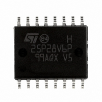
M25P128-VMF6P NUMONYX, M25P128-VMF6P Datasheet - Page 22

M25P128-VMF6P
Manufacturer Part Number
M25P128-VMF6P
Description
IC FLASH 128MBIT 50MHZ 16SOIC
Manufacturer
NUMONYX
Series
Forté™r
Datasheet
1.M25P128-VME6TGB.pdf
(47 pages)
Specifications of M25P128-VMF6P
Format - Memory
FLASH
Memory Type
FLASH
Memory Size
128M (16M x 8)
Speed
50MHz
Interface
SPI, 3-Wire Serial
Voltage - Supply
2.7 V ~ 3.6 V
Operating Temperature
-40°C ~ 85°C
Package / Case
16-SOIC
Cell Type
NOR
Density
128Mb
Access Time (max)
8ns
Interface Type
Serial (SPI)
Boot Type
Not Required
Address Bus
1b
Operating Supply Voltage (typ)
3.3V
Operating Temp Range
-40C to 85C
Package Type
SO W
Sync/async
Synchronous
Operating Temperature Classification
Industrial
Operating Supply Voltage (min)
2.7V
Operating Supply Voltage (max)
3.6V
Word Size
8b
Number Of Words
16M
Supply Current
8mA
Mounting
Surface Mount
Pin Count
16
Lead Free Status / RoHS Status
Lead free / RoHS Compliant
Other names
Q2855929
Q3097367
Q3097367
Available stocks
Company
Part Number
Manufacturer
Quantity
Price
Part Number:
M25P128-VMF6P
Manufacturer:
ST
Quantity:
20 000
Company:
Part Number:
M25P128-VMF6PB
Manufacturer:
CIRRUS
Quantity:
320
Part Number:
M25P128-VMF6PB
Manufacturer:
ST
Quantity:
20 000
Company:
Part Number:
M25P128-VMF6PB,M25P128-VMF6TP
Quantity:
70
6.4
6.4.1
6.4.2
6.4.3
6.4.4
22/47
Read status register (RDSR)
The Read Status Register (RDSR) instruction allows the Status Register to be read. The
Status Register may be read at any time, even while a Program, Erase or Write Status
Register cycle is in progress. When one of these cycles is in progress, it is recommended to
check the Write In Progress (WIP) bit before sending a new instruction to the device. It is
also possible to read the Status Register continuously, as shown in
Table 6.
The status and control bits of the Status Register are as follows:
WIP bit
The Write In Progress (WIP) bit indicates whether the memory is busy with a Write Status
Register, Program or Erase cycle. When set to 1, such a cycle is in progress, when reset to
0 no such cycle is in progress.
WEL bit
The Write Enable Latch (WEL) bit indicates the status of the internal Write Enable Latch.
When set to 1 the internal Write Enable Latch is set, when set to 0 the internal Write Enable
Latch is reset and no Write Status Register, Program or Erase instruction is accepted.
BP2, BP1, BP0 bits
The Block Protect (BP2, BP1, BP0) bits are non-volatile. They define the size of the area to
be software protected against Program and Erase instructions. These bits are written with
the Write Status Register (WRSR) instruction. When one or more of the Block Protect (BP2,
BP1, BP0) bits is set to 1, the relevant memory area (as defined in
protected against Page Program (PP) and Sector Erase (SE) instructions. The Block Protect
(BP2, BP1, BP0) bits can be written provided that the Hardware Protected mode has not
been set. The Bulk Erase (BE) instruction is executed if, and only if, all Block Protect (BP2,
BP1, BP0) bits are 0.
SRWD bit
The Status Register Write Disable (SRWD) bit is operated in conjunction with the Write
Protect (W/V
(W/V
Register Write Disable (SRWD) bit is set to 1, and Write Protect (W/V
this mode, the non-volatile bits of the Status Register (SRWD, BP2, BP1, BP0) become
Status Register Write Protect
SRWD
PP
b7
) signal allow the device to be put in the Hardware Protected mode (when the Status
Status register format
PP
) signal. The Status Register Write Disable (SRWD) bit and Write Protect
0
0
BP2
BP1
Block Protect Bits
Write Enable Latch Bit
BP0
Table
Figure
PP
) is driven Low). In
Write In Progress Bit
WEL
2) becomes
11.
WIP
b0


